
Abstract
We have successfully demonstrated the room-temperature continuous-wave operation of GaN-based vertical-cavity surface-emitting lasers (VCSELs) with all-dielectric reflectors, which were fabricated using epitaxial lateral overgrowth. The VCSELs exhibited a threshold current of 8 mA and a threshold voltage of 4.5 V at a lasing wavelength of 446 nm. The maximum output power was 0.9 mW for an 8-µm-diameter current aperture, which was made possible because of the high thermal conductivity of the GaN substrate.
Export citation and abstract BibTeX RIS
Gallium nitride (GaN)-based optoelectronic devices such as light-emitting diodes and edge-emitting lasers are widely used for lighting and optical data storage.1,2) In addition, there has recently been considerable interest in the development of GaN-based vertical-cavity surface-emitting lasers (VCSELs).3–18) Such VCSELs are promising optical sources for displays, laser printers, and biomedical devices because they are capable of single longitudinal-mode emission, they exhibit a low threshold current, they can form circular spots, and they can be patterned into two-dimensional arrays. A number of different structures have already been fabricated using all-dielectric distributed Bragg reflectors (DBRs)4,7,8,13–17) or a mixture of semiconductor and dielectric DBRs (hybrid DBR structure).3,9–12) However, all of these approaches have issues, such as achieving a high-power continuous-wave (CW) output at room temperature, fabricating high-reflectance semiconductor DBRs, precise control of the cavity length, and efficient heat management. Lu et al. reported a room-temperature CW output in the violet region for a GaN-based VCSEL using a hybrid DBR structure,10) in which the semiconductor AlN/GaN DBR was grown by metal organic chemical vapor deposition (MOCVD). The device had a threshold current density of 12.4 kA/cm2 and an output power of less than 40 µW. The weak output was considered to be due to the low reflectance of the semiconductor DBR. There is a large lattice mismatch between the AlN and GaN layers that constitute the DBR, and this gives rise to cracks that reduce the reflectance. Although all-dielectric DBRs can exhibit a high reflectance, they are associated with different types of problem. To form an optical cavity using such DBRs, it is necessary to remove the GaN substrate using a method such as chemical mechanical polishing (CMP). However, with CMP, it is difficult to control the cavity length and flatten the exit surface. Deviations from the designed optical cavity length and the tilting exit surface lead to increases in internal and mirror losses. Moreover, during the CMP process, a Si wafer is normally used as a support substrate, and since its thermal conductivity is lower than that of GaN, excessive heating of the DBR can occur. Kasahara et al. reported GaN-based VCSELs using an all-dielectric DBR structure.15) They first produced an n-type GaN layer, the active layer, and p-type GaN layers on a GaN substrate. They formed bottom dielectric DBRs and bonded the Si wafer. They then used CMP to remove the substrate and control the cavity length. Finally, they formed top dielectric DBRs. Their devices exhibited CW blue emission with a threshold current density of 3.0 kA/cm2, a threshold voltage of 3.3 V, and a maximum output power of 0.7 mW. The fact that the output power was not high despite the low threshold current density may indicate that the low thermal conductivity of the Si substrate may have led to excessive heating. Okur et al. proposed a structure in which an optical cavity was formed on bottom dielectric DBRs embedded in GaN by epitaxial lateral overgrowth (ELO) on a sapphire substrate.18) The ELO method enables the incorporation of high-reflectance dielectric DBRs. It also allows fabrication steps such as polishing and bonding to be eliminated. However, for the device reported by Okur et al., lasing occurred only under optical excitation at violet wavelengths.
In the present study, in order to fabricate high-reflectance DBRs, control the cavity length, and manage heat generation, the ELO method was used in combination with an n-type GaN substrate. The thermal conductivity of n-type GaN is higher than that of the sapphire or Si substrates used during CMP, and the reduced thermal impedance is expected to lead to improved optical characteristics. Moreover, ELO allows the precise control of the cavity length and the formation of high-reflectance dielectric DBRs. Here, we report CW blue emission from electrically pumped GaN-based VCSELs fabricated using ELO for the first time.
Figure 1 shows a schematic illustration of the VCSEL device structure. All of the epitaxial layers were grown by MOCVD. The bottom DBR consisted of 14.5 SiO2/SiNx bilayers and was deposited directly on the GaN substrate. It was patterned following growth and then embedded in n-type GaN using ELO. The thickness of the n-type GaN layer was controlled to be precisely 4 µm on the basis of pre-evaluated growth rate. The active layer consisted of a two-pair GaInN (6 nm)/GaN (10 nm) multiple quantum well (MQW) structure and was covered by a p-type GaN layer. Transmission and scanning electron microscopy observations confirmed that the bottom DBR did not become detached from the GaN substrate. An SiO2 layer was deposited on the p-type GaN layer and then patterned to form a circular current aperture of 8 µm diameter. Following the deposition of an indium tin oxide (ITO) p-type ohmic contact, a top DBR structure consisting of 12 Ta2O5/SiO2 bilayers was deposited. The wafer was lapped to a thickness of approximately 80 µm, and the VCSEL chip was mounted on a ϕ5.6 can package with a junction-up configuration.
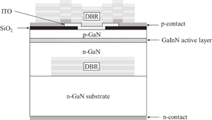
Fig. 1. Schematic illustration of ELO GaN-based VCSEL structure.
Download figure:
Standard image High-resolution imageFigure 2 shows the current–light output (I–L) and current–voltage (I–V) characteristics of the device under room-temperature CW operation. The threshold current and threshold voltage were 8 mA and 4.5 V, respectively, and the threshold current density was estimated to be 16 kA/cm2. A maximum output power of 0.9 mW was obtained. This is the highest output power ever reported for a GaN-based VCSEL with an 8 µm aperture diameter, and is considered to be due to the high thermal conductivity of the n-type GaN. Furthermore, in the figure, it can be seen that the I–L curve has a kink at a current value of about 17 mA due to multimode lasing.
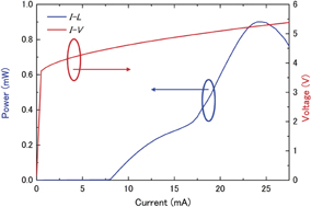
Fig. 2. Output power and voltage as functions of injection current at room temperature.
Download figure:
Standard image High-resolution imageFigure 3 shows the emission spectra for driving currents of 7 and 8 mA. The spectral longitudinal mode spacing measured below the threshold current was approximately 6.7 nm, and by using a group refractive index of 3.3, the optical cavity length was estimated to be 4.5 µm, which was close to the n-GaN thickness of 4 µm. The slight difference may be due to small variations in group refractive index. When the injection current was increased to 8 mA, the intensity of the peak at 446.0 nm was selectively enhanced and the full width at half maximum (FWHM) was measured to be 0.05 nm. However, since this FWHM corresponds to the wavelength resolution of the spectrum analyzer (ADCMT 8341), it is likely that the true FWHM was smaller.
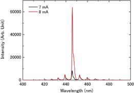
Fig. 3. Emission spectra for two different injection currents.
Download figure:
Standard image High-resolution imageFinally, the near-field pattern for an injection current of 10 mA is shown in Fig. 4. The bright blue region (lasing region) is circular and has a diameter of 8 µm, which indicates that the VCSEL had a flat surface and that the contact resistance was uniform within the 8-µm-diameter current aperture.

Fig. 4. Near-field pattern for device operated above threshold current.
Download figure:
Standard image High-resolution image
In summary, we used ELO to fabricate GaN-based VCSELs and achieved room-temperature CW lasing at 446.0 nm for the first time. The threshold current and maximum output power were 8 mA and 0.9 mW, respectively. To the best of our knowledge, this is the highest output power ever reported for a pure blue VCSEL. We believe that this can be attributed to the combined use of ELO and a GaN substrate.
Acknowledgments
The authors thank Mr. Jyokawa and Mr. Ansai for assistance with device fabrication, and Dr. R. Koda, Dr. Y. Takiguchi, and Dr. S. Kono for technical support and helpful discussions.