
Abstract
Dislocations in n- and p-type substrates as well as in epitaxial layers (epilayers) were clearly identified using a photoluminescence (PL) imaging technique. Dislocations in epilayers show large/small bright spots or lines in infrared PL images, which correspond to threading screw/edge dislocations (TSDs/TEDs) or basal plane dislocations (BPDs), respectively. In contrast, dislocations in substrates exhibit large/small dark spots or dark lines in infrared PL images, corresponding to TSDs/TEDs or BPDs, respectively. These different features (bright/dark contrast) of dislocations may originate from the different densities of point defects or impurities.
Export citation and abstract BibTeX RIS
SiC is a promising semiconductor material for high-voltage and high-temperature devices. Through recent progress in crystal growth and device technology, the mass production of 600–1700 V SiC power devices has started. For ultrahigh-voltage (>10 kV) applications, where SiC bipolar devices are attractive owing to the effect of conductivity modulation, 10–20 kV class PiN diodes and thyristors have been demonstrated.1–5) However, the potential of SiC bipolar devices is severely hampered by the generation and expansion of Shockley-type stacking faults originating from basal plane dislocations (BPDs).6,7) Moreover, some TSDs in substrates can work as the source of Frank-type stacking faults or carrot defects, resulting in the degradation of electrical characteristics.8,9) Thus, it is important to understand the behavior of dislocations in SiC epitaxial layers and substrates.
Up to now, various methods, such as cross-sectional transmission electron microscopy (TEM), molten KOH etching, X-ray topography, photoluminescence (PL) mapping, and PL imaging, have been utilized for detecting extended defects in SiC.10–14) In particular, PL imaging is a high-speed and nondestructive method for detecting dislocations in SiC. Isono et al. reported a pioneering work on the PL imaging of high-resistivity 6H-SiC wafers.12) In most cases, however, this technique has been almost exclusively applied to n-type epilayers.15–18) In this study, we investigated dislocations in n- and p-type 4H-SiC epilayers as well as in substrates using PL imaging. Dislocations were clearly identified not only in epilayers but also in substrates by infrared PL imaging.
The samples used in this study were n- and p-type 4H-SiC (0001) 4 or 8° off-axis epilayers with various thicknesses (30–270 µm) and commercial, heavily doped n- and p-type substrates. The doping concentrations of n- and p-type epilayers were in the range of 1014–1017 cm−3. To enhance dislocation contrasts in PL images from epilayers, the Z1/2 center,19) the carrier lifetime killer,20) was reduced by high-temperature oxidation.17,21) The typical oxidation condition was 1400–1500 °C for 24 h. Note that no such treatment was applied to substrates. In the PL imaging measurements, a filtered Hg–Xe UV lamp was employed as an excitation source. The filter of the excitation source (excitation filter) was selected from three filters, which are a wide band-pass (λ: 270–380 nm) or two types of band-pass (λ: 313 nm, 365 nm), depending on sample thickness (typically a wide band-pass filter was used). The penetration depths of the emission lines at 365 and 313 nm are approximately 100 and 4 µm, respectively.22) An area of 5 × 8 mm2 was illuminated, where the power density was about 0.90 W/cm2. Part of the excited region (660 × 660 µm2) was imaged using a back-illuminated deep depletion-type imaging charge-coupled device with a long-pass (>750 nm) or a band-pass (900 ± 5 nm) filter attached to an optical microscope. All the PL images were acquired at room temperature. The exposure time was changed from 500 ms to 10 s (typically 1 s) for one image (660 × 660 µm2), depending on the sample conditions. We also measured PL spectra from selected areas at room temperature. The excitation source for the recording of PL spectra was a 25 mW He–Cd laser (λ: 325 nm). PL was dispersed with a grating monochromator and detected using a charge-coupled device array. The spot diameter of the laser was about 10 µm. Evidence of locations and types of dislocations was obtained by molten KOH etching for epilayers and KOH+Na2O2 etching for substrates.23) The etching temperature and duration for epilayers and substrates were 450 °C 4 min and 500 °C 1 min, respectively. Etch pits were observed by Nomarski optical microscopy.
Figure 1(a) shows the infrared (900 ± 5 nm) PL image obtained from a thick (186 µm) n-type epilayer (donor concentration: Nd = 2 × 1014 cm−3) and Fig. 1(b) shows etch pits of the same location. Large or small bright spots and bright lines were observed and identified as threading screw/edge dislocations (TSDs/TEDs) and BPDs, respectively. This result is consistent with previous reports.14,24) Figure 1(c) shows the infrared (>750 nm) PL image of a thick (147 µm) p-type epilayer (acceptor concentration: Na = 5.6 × 1014 cm−3) and Fig. 1(d) shows the etch pits of the same location. In a similar manner, large or small bright spots and lines correspond to TSDs or TEDs and BPDs, respectively. Thus, dislocations in both n- and p-type epilayers are detected as bright spots or lines in infrared PL images.
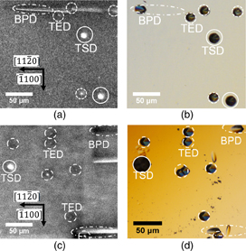
Fig. 1. RT PL images of (a) an n-type epilayer taken with a band-pass filter (900 ± 5 nm) and (c) a p-type epilayer taken with a long-pass filter (>750 nm). (b) and (d) etch pits of the same location of n- and p-type epilayers, respectively. Large (∼10 µm)/small (∼2 µm) bright spots and bright lines correspond to TSDs/TEDs and BPDs, respectively.
Download figure:
Standard image High-resolution imageIn contrast, Fig. 2(a) depicts the infrared (>750 nm) PL image acquired from an n-type substrate, and Fig. 2(b) shows the etch pits formed by molten KOH+Na2O2 etching of the same location. Large/small dark spots and dark lines correspond to TSDs/TEDs and BPDs, respectively. The same result was observed in p-type substrates and confirmed that, large/small dark spots and dark lines correspond to TSDs/TEDs and BPDs (images not shown), respectively. Therefore, the appearance of dislocations in substrates (dark contrast of dislocations) is different from that in epilayers (bright contrast). The appearance of dislocations in infrared PL images is summarized in Table I.

Download figure:
Standard image High-resolution image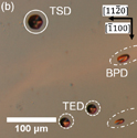
Fig. 2. (a) RT PL images of an n-type substrate with a long-pass filter (>750 nm). (b) KOH+Na2O2 etch pits of the same location. Large (∼25 µm)/small (∼10 µm) dark spots and lines have a one-to-one relationship to TSDs/TEDs and BPDs, respectively.
Download figure:
Standard image High-resolution imageTable I. Appearance of dislocations in the near-infrared PL images at room temperature.
| Appearance in PL images | Densities of impurities and point defects | ||
|---|---|---|---|
| TSD/TED | BPD | ||
| Epilayer | Bright spot | Bright line | Low |
| Substrate | Dark spot | Dark line | High |
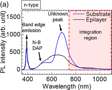
To investigate radiative carrier recombination, we measured PL spectra at room temperature. Figures 3(a) and 3(b) show PL spectra of n- and p-type epilayers/substrates, respectively. These PL spectra were measured in the dislocation-free regions of the samples. In these spectra, substrates and epilayers exhibit a PL peak near 390 nm (the band edge emission) and 500 nm (the nitrogen donor-boron acceptor recombination-related emission).25,26) Although a broad peak at 680 nm was observed, the origin of this peak is not clear at present. Since most images were acquired by using a long-pass filter (>750 nm) in a PL imaging experiment, we compare PL from substrates with that from epilayers by integrating the PL intensity in the wavelength range from 750 to 1100 nm (indicated by a red square in Fig. 3). For both n- and p-type, the total PL intensity of this range (near-infrared region) in substrates is larger than that in epilayers.

Download figure:
Standard image High-resolution image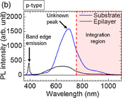
Fig. 3. RT PL spectra of (a) n- and (b) p-type epilayers/substrates. PL spectra were acquired at dislocation-free areas in epilayers and substrates.
Download figure:
Standard image High-resolution imageOn the basis of the appearance of dislocations in epilayers and substrates, both (bright and dark) features of dislocations can be observed when we take a PL image of a relatively thin epilayer, because PL signals from the epilayer and the underlying substrate can be simultaneously acquired. Figures 4(a) and 4(b) show the infrared (>750 nm) PL image of a 30-µm-thick n-type epilayer grown on an n-type substrate at the same location but with different filters. The penetration depth of the UV source is deeper as the excitation wavelength becomes longer. Figure 4(a) represents the image observed with a 313 nm excitation filter, where bright lines and a bright spot are observed. Figure 4(b) represents the image observed with a 365 nm excitation filter, where some dark lines and spots emerged in addition to bright lines and spots. Bright spots are observed inside dark spots, and a bright spot is observed at the end of a dark line. The former means the replication of TSD (TSD→TSD) or TED (TED→TED), and the latter indicates BPD-to-TED conversion in the epitaxial growth. The schematic illustration of the appearance near a dislocation in a SiC epilayer/substrate structure is shown in Fig. 4(c). Thus, the conversion and replication of dislocations in SiC epilayers can be examined by infrared PL imaging.
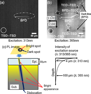
Fig. 4. RT PL images of a relatively thin (30 µm) n-type epilayer taken with a long-pass filter (>750 nm) at the same location. The filter of the excitation source was (a) 313 nm, (b) 365 nm. The penetration depth becomes deeper as the wavelength of filter becomes longer. Bright spots are observed inside dark spots, and a bright spot is observed at the end of a dark line. The former means replication of TSD (TSD→TSD) and TED (TED→TED), and the latter shows BPD-to-TED conversion. (c) Cross-sectional schematic illustration of the appearance of dislocations in PL images.
Download figure:
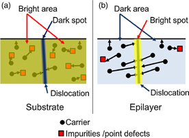
Standard image High-resolution imageThese PL images can be interpreted by taking into account the different recombination paths in epilayers and substrates as follows. Figures 5(a) and 5(b) show schematic illustrations of carrier recombination paths in substrates and epilayers, respectively. Since the SiC substrates contain high densities of point defects27) and impurities (including dopants), photoexcited carriers will mainly recombine at these defects and impurities. These recombination sites exist in the substrates almost uniformly, and some of them provide radiative recombination, leading to bright PL images in photoexcited areas. Dislocations behave basically as nonradiative recombination centers. As a result, background PL images (entire photoexcited region) become bright, while dark areas appear near the dislocations. In high-quality and lightly doped SiC epilayers, however, the densities of point defects and impurities are much lower, leading to a relatively long carrier lifetime. Excited carriers can diffuse in a relatively long distance and reach dislocations. Although dislocations should behave basically as nonradiative recombination centers, some carriers show radiative recombination via localized states of dislocations. Thus, the background PL images from epilayers are relatively dark, while bright PL images appear near the dislocations. To validate this model, the origins of the infrared PL as well as the PL near the dislocation cores must be clarified.
Fig. 5. Schematic illustrations of carrier recombination path in (a) substrate and (b) epilayer. Dislocations basically behave as nonradiative recombination centers. However, the carrier lifetime in the epilayer is much longer than that in the substrate (typically 1 µs or longer). Then the excited carriers can diffuse in a relatively long distance and reach dislocations, and some of them show radiative recombination via localized states of dislocations.
Download figure:
Standard image High-resolution image
In summary, PL imaging is an effective method for detecting dislocations, regardless of the conduction types (n-/p-type) and structures (epilayers, substrates, epilayer/substrate). In high-quality epilayers, dislocations can be detected as bright spots (TSDs, TEDs) or bright lines (BPDs) in infrared PL images. On the other hand, dislocations in substrates can be detected as dark spots or dark lines. These differences may originate from the difference in densities of point defects and impurities.
Acknowledgements
This work was supported by the Funding Program for World-Leading Innovative R&D on Science and Technology (FIRST Program) and by a Grant-in-Aid for Scientific Research (21226008) from the Japan Society for the Promotion of Science.