Abstract
Many power switching devices are used in hybrid vehicles (HVs) and electric vehicles (EVs). To improve the efficiency of HVs and EVs, better performance characteristics than those of Si power devices, for example, lower on-resistance, higher speed, higher operation temperature, are required for the power devices. GaN power devices are promising candidates for satisfying the requirements. A lateral GaN power device with a blocking voltage of 600 V and a vertical GaN power device with a blocking voltage of 1200 V are suitable for medium power applications for sub systems and high-power applications for the drive of main motors, respectively. Power device applications in HVs and EVs and the current status of the GaN power device are presented. The reliability of the GaN power device is also discussed.
Export citation and abstract BibTeX RIS
1. Introduction
Since the final decade of the 20th century, dwindling oil reserves and climate change have been viewed as serious global problems. For this reason, methods for reducing the amount of energy used have become the focus of considerable attention. Automobiles are consuming a large amount of energy globally. Therefore, the improvement of the efficiency of power sources in automobiles is being strongly pursued. One of the solutions for this is to change the power source from fossil fuels to electric power. The first hybrid vehicle, Prius, has been on sale since 1997. Subsequently, many automotive companies in the world began developments of hybrid vehicles (HVs) and electric vehicles (EVs). Nowadays, many kinds of HVs are sold throughout the world. In the HV and EV systems, power electronics plays important roles because the power electronics defines the efficiency of these systems. One area that has received particular attention is the field of power devices, because power devices directly control the flow of electrical energy. The present HV and EV systems use Si power devices, that is, insulated gate bipolar transistors (IGBTs) and MOSFETs. The performance of Si power devices is still evolving, but it will be limited by the Si material characteristics. Therefore, to improve the efficiency of future HV and EV systems, power devices with better performance than Si power devices are strongly required. The wide-band-gap semiconductors GaN and SiC are promising post-Si power device materials. Power devices consisting of GaN or SiC have recently started to approach practical applicability. GaN power devices have the highest potential among Si, SiC, and GaN and suitable characteristics for HV and EV applications. We have been developing GaN power devices for automotive applications. In this paper, the power electronics used in HV and EV systems and requirements of the new devices are first presented, and then the current status and issues of GaN power devices for automotive applications are described.
2. Power electronics in HVs
Many power modules are used in the HV system as shown schematically in Fig. 1. The power electronics used in HVs and EVs is basically the same except for the engine. These power modules are divided into two categories by power level: high-power modules used to drive the main motor, and medium- and low-power modules used to drive the subsystems.
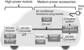
Fig. 1. Power modules used in HV. The power modules can be divided into two categories by control power level: high-power modules and medium- and low-power modules.
Download figure:
Standard image High-resolution imageThe high-power modules for controlling the main motor consist of a bidirectional DC–DC converter and an inverter. These circuits are shown in Fig. 2. They are contained in the power control unit (PCU), as shown in Fig. 2, and are water cooled. The battery voltage is raised to the motor source voltage by the DC–DC converter and then the source voltage is supplied to the motor through the inverter. The boost ratio changes depending on the driving condition. The maximum voltage is 650 V. The DC–DC converter is also used as a buck converter so the generator can charge the battery. The maximum output power of the main motor of Prius is 60 kW; in the case of a large sedan, the required motor power is over 150 kW. Therefore, the DC–DC converter and the inverter must control such a high power. Moreover, the modules must provide guaranteed operation under any driving condition, so a large current capacity, such as over 200 A per chip, is required for these power devices. In the high-power modules, Si-IGBTs and pin diodes, which have sufficient current capacity and reliability, are now used. The breakdown rating of the devices is 1.25 kV owing to the maximum source voltage of 650 V. The efficiency of the inverter is very high (>98%) under the maximum output condition. However, there are few opportunities to use the maximum power under general driving conditions. The average power used for driving will be lower than half the maximum output power. The efficiency of Si-IGBTs is lower under low-power conditions than under high-power conditions because of the junction voltage, which are bipolar device characteristics. Therefore, unipolar devices such as MOSFETs with sufficient low on-resistance are required to improve the total efficiency of the inverter in next-generation systems. Moreover, in pulse width modulation (PWM) control for the inverter, high carrier frequency reduces ripples in the output voltage, which improves the motor efficiency. High-speed MOSFETs will make the high carrier frequency possible. High-speed performance of the power device is also desirable in the DC–DC converter. In the present DC–DC converter, the switching frequency is 5–10 kHz, which requires a large capacitor and a large inductor. Higher frequency operation permits the use of a small capacitor and a small inductor.
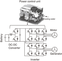
Fig. 2. Circuits of an inverter and a DC–DC converter used to control the main motor. These modules are installed into the power control unit and water-cooled.
Download figure:
Standard image High-resolution imageThe main problem of the high power module is the large amount of heat generated which gives rise to a need for a water cooling system for the power control unit. If power devices were capable of high-temperature operation, for example, above 200 °C, we could simplify the cooling system. High-temperature operation is another required performance of the new power device.
Another category in HV power electronics systems is medium-power applications. There are many electrically driven accessories in HV systems. The highest power output accessory is an air conditioner, the power of which is 5–6 kW. A compressor in the air conditioner is driven by an inverter with the battery voltage of 200–300 V. Other accessories driven by the battery voltage are the inverters for AC sources for home electric appliances, which will be useful in times of disaster, and a buck converter for 12 V accessories. A charging system is also a medium-power application. The charging system is used in EVs and plug-in HVs (PHVs). The block diagram of the charging system for a home power source is shown in Fig. 3. The AC voltage is converted to DC voltage using an AC–DC converter, which is power factor correction (PFC) converter. The DC voltage is converted to high frequency and the electric energy is transferred to a rectifier through an isolation transformer, and the battery is charged. The electric power is about 3 kW. Another charging system being developed is a wireless charging system, which uses resonant inductive coupling, and the frequency used will be over 10 MHz. High-power and high-frequency devices are required for the high frequency amplifier in this system. The required breakdown voltage is 400–600 V depending on the battery voltage. The suitable performance of devices for these applications is high-frequency operation because it induces high efficiency and small size of the system. Therefore, high-speed and low-on-resistance devices are required for these medium-power applications. For these medium power applications, Si-MOSFETs are now used as power devices. Therefore, low cost and high performance are very important factors for the new devices.
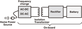
Fig. 3. Block diagram of a battery charging system from a home power source.
Download figure:
Standard image High-resolution imageTotal loss in the medium-power modules is not very high compared with that in high-power modules. However, electric power loss directly affects the driving distance, especially in the case of EVs. Therefore, loss reduction is very important not only in high-power applications but also in medium-power applications.
3. GaN power devices
Before the year 2000, it was widely recognized that SiC would replace Si as a high-performance power-device material. However, epoch-making research was presented in 2001, when a team from the University of California at Santa Barbara and Yale University reported the high performance of an AlGaN/GaN-based high-voltage transistor.1) Its breakdown voltage and specific on-resistance were 1.2 kV and 2 mΩ·cm2, respectively. This impressively high breakdown voltage led to a surge of interest in GaN as an alternative to SiC for next-generation power devices.
Over the past decade, the performance of GaN power devices has been rapidly improving. There are two types of devices currently being developed, which have the lateral and vertical structures. At present, the mainstream GaN power devices have a lateral structure, and many vendors have announced plans for the commercialization of such devices.2) The lateral GaN power device with a blocking voltage of 600 V has high performance characteristics, such as low on-resistance and high-speed response compared with Si power MOSFETs. These characteristics are highly suitable for the medium-power applications in HVs. On the other hand, although the high potential of GaN for vertical devices has been predicted,3) the progress of the vertical devices is slower than that of the lateral devices. However, the vertical devices have recently been attracting this researcher's attention. In this section, the current status of the vertical and lateral GaN power devices is presented.
3.1. Vertical GaN power devices
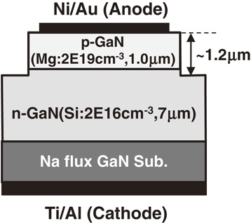
The vertical structure has the advantages of small chip size, easy wiring, high breakdown voltage, and current-collapse-free operation. These characteristics are highly suitable for high-power applications. We started the development of vertical GaN power devices in 2004. The first developed device structure is shown in Fig. 4. It is similar to the structure of a double diffused Si MOSFET.4) The electron current flows through the AlGaN/GaN heterojunction and an aperture at the center of the p-GaN layer. The p-GaN layer plays the role of a current blocking layer during the off-state. We employed an insulated gate, which allows higher voltage to be applied to the gate electrode and the gate leakage current to be reduced. Figure 5 shows the process flow for the device fabrication. First, a 3-µm-thick n−-GaN layer (Si: 1 × 1016 cm−3), a 0.1-µm-thick p-GaN layer (Mg: 3 × 1019 cm−3), a 10-nm-thick AlN layer, and a 50-nm-thick undoped-GaN layer were grown on a c-plane n+-type GaN substrate by metal organic chemical vapor deposition (MOCVD), as shown in Fig. 5(a). Next, the undoped-GaN/AlN/p-GaN was dry-etched by inductively coupled plasma (ICP) dry etching with Cl2 gas using a SiO2 mask [Fig. 5(b)]. After the removal of the mask, a 0.3-µm-thick n−-GaN layer (Si: 1 × 1016 cm−3) and a 15-nm-thick Al0.25Ga0.75N layer were regrown [Fig. 5(c)]. During this regrowth process, the AlN layer suppressed the upward diffusion of the Mg atoms in the p-GaN layer as well as the mass transport from the surface to the aperture region. The source regions were formed by Si ion implantation at an acceleration energy of 40 keV with a dosage of 3 × 1015 cm−2 and by activation annealing at 1000 °C for 20 min with SiO2-encapsulated layer. A 50-nm-thick SiO2 gate insulator layer was deposited by low-pressure chemical vapor deposition (LPCVD). A phosphorous-doped polycrystalline silicon (poly-Si) film was deposited as the gate electrode by LPCVD, followed by activation annealing at 850 °C for 20 min in nitrogen ambient. At the same time, Mg in the p-GaN layer was activated. The poly-Si gate electrode was defined by dry etching. A 500-nm-thick SiO2 interlayer was deposited by plasma CVD and the contact holes were formed by dry etching. Finally, the source and drain electrodes Ti/Al were formed by electron beam evaporation [Fig. 5(d)]. The operation mode of this device was normally-on with the threshold voltage −16 V, because the gate channel was the AlGaN/GaN heterostructure. The ID–VD characteristics are shown in Fig. 6. This was the first demonstration of the vertical GaN transistor.

Fig. 4. Schematic cross-sectional view of the vertical insulated gate AlGaN/GaN HFET.
Download figure:
Standard image High-resolution image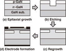
Fig. 5. Process flow for fabrication of the vertical GaN device.
Download figure:
Standard image High-resolution image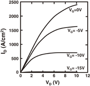
Fig. 6. ID–VD characteristics of the fabricated vertical GaN device. The gate voltage range is from 0 to −15 V.
Download figure:
Standard image High-resolution imageAnother device structure, that of a conventional trench MOSFET, was also examined as shown in Fig. 7.5) Trench MOSFETs are popular for Si and SiC power devices. However, for GaN, it was unknown whether or not the trench sidewall of GaN could be used as a gate channel. The trench was first made by ICP dry etching. The trench shape after dry etching was a V-shaped groove and the sidewall of the trench was rough, as shown in Fig. 8(a). We found that wet etching using tetramethylammonium hydride (TMAH) modifies the dry-etched sidewall to be atomically flat as shown in Fig. 8(b). The GaN trench MOSFET made by this novel trench fabrication technology was demonstrated.5) Other reports on the vertical GaN devices fabricated on GaN substrates have also been published.6–10) However, the device performance is yet far from the desired performance.

Fig. 7. Schematic cross-sectional view of the trench gate MISFET.
Download figure:
Standard image High-resolution image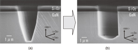
Fig. 8. (a) SEM image of the trench shape after dry etching. (b) SEM image of the trench shape after wet etching subsequent to dry etching.
Download figure:
Standard image High-resolution imageThrough the fabrication of the vertical GaN devices, we have revealed the development issues as summarized in Fig. 9. The main issue is the quality of the GaN substrate. GaN substrates for blue laser applications made by hydride vapor phase epitaxy (HVPE) have been commercially available since the early 2000s. We evaluated the GaN substrates by forming Schottky barrier diodes on these GaN substrates, and observed high leakage characteristics under high reverse voltage. Recently, new approaches to fabricating high-quality GaN substrates have been developed. They are liquid-phase growth technologies: the ammonothermal method11–13) and the Na flux method.14–17) We evaluated a GaN substrate made by the Na flux method. It was evaluated by measuring the leakage current and the leakage points on pn diodes fabricated on the Na flux GaN substrate.18) The evaluated diode structure and the leakage current are shown in Fig. 10. This diode had a breakdown voltage exceeding 1000 V. We have examined leakage points using an emission microscope. Four emission points, as shown in Fig. 11(a) with arrows, were observed under 800 V reverse voltage. The emissions had broad spectra indicating that the emissions were due to hot electrons in the leakage currents. After the observation, the diode was etched to form etch pits originating from the dislocations in the epitaxial layer, using a mixture of acids ( , 250 °C). The etched surface is shown in Fig. 11(b). We compared Fig. 11(a) with Fig. 11(b) in detail and found that the leakage points did not coincide with any etch pits. Moreover, the origins of the etch pits were examined by cross-sectional transmission electron microscopy (TEM). Edge and mixed (edge + screw) dislocations were observed beneath the etch pits. These results suggest that the edge and mixed dislocations are not the cause of the leakage current, which is consistent with previous reports on the electric characteristics of the dislocations.19,20) Although pure screw dislocations were not found in this diode sample, the screw dislocations will be conductive and become killer dislocations for high-voltage applications. However, the origin of the leakage current in Fig. 10 has remained unclear. We now estimate, from measurements of other samples, that the origin is inclusions or dust near the pn junction that are included during epitaxial growth. Our evaluation indicates that the edge and mixed dislocations do not affect the leakage current at high reverse voltage and recent GaN substrates are of sufficient quality for research on high-voltage vertical devices. Recent research on diodes has also revealed that the quality of GaN substrates made by HVPE has become sufficiently high to apply them to high-voltage devices.21–23) However, the whole GaN substrate area does not yet have uniform quality. Therefore, the remaining issues of GaN substrate development are large size with uniformly high quality and dislocation reduction.
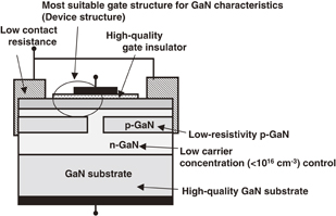
Fig. 9. Subjects in development of the vertical GaN device.
Download figure:
Standard image High-resolution image
Download figure:
Standard image High-resolution image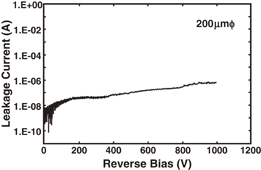
Fig. 10. Structure of the diode used to evaluate the GaN substrate made by Na flux method and its leakage characteristics.
Download figure:
Standard image High-resolution image
Download figure:
Standard image High-resolution image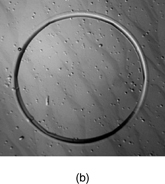
Fig. 11. (a) Images of the emissions caused by leakage current. Arrows indicate the emission points. (b) Optical microscopy image of etch pits on the surface of the diode.
Download figure:
Standard image High-resolution imageThe next issue is low n-type doping control of an epitaxial layer. Figure 12 shows the relationship between carrier concentration and breakdown voltage for drift layer thicknesses. We can see that carrier concentrations less than 1 × 1016 cm−3 are required for breakdown voltages over 1 kV. To obtain a low-carrier-concentration and low-resistive-drift layer, a high-quality crystal with few contaminations is necessary. However, carbon atoms, the concentration of which is about 1 × 1016 cm−3, are included in epitaxial layers grown by MOCVD. These carbon atoms will compensate Si donors and result in a highly resistive epitaxial layer. The carbon atoms mainly come from trimethylgallium (TMG), the Ga source. Therefore, it is difficult to reduce carbon contamination below 1 × 1016 cm−3, and epitaxial technology for growing highly pure GaN is essential for high-voltage devices. The next issue is related to p-GaN. It is difficult to fabricate a low-resistance and stable p-type GaN layer. A low-resistance p-type layer is needed to ensure avalanche ruggedness of the device, as mentioned in Sect. 4. For the issue of low contact resistance in Fig. 9, ion implantation is an effective method for producing a high-carrier-density thin layer under the ohmic electrode, which induces low contact resistance. Ion implantation of n-type dopants, Si and Ge, to GaN has been investigated,24,25) and good activations have been obtained. On the other hand, activations of ion-implanted p-type dopants, Mg and Be, are difficult.26,27) If p-type ion implantation is achieved, it will simplify the fabrication process of the vertical GaN device. The final issue in Fig. 9 is the gate structure, which determines the device characteristics. A gate structure that is normally-off and has low channel resistance must be developed. The issues shown in Fig. 9 are now being investigated, but they are not yet at a sufficient level since some of them are issues peculiar to vertical devices. To approach the theoretical performance limit, these subjects must be overcome at high levels.
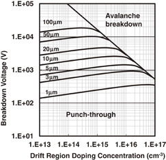
Fig. 12. Breakdown voltage vs drain region doping concentration for each drift layer thickness from 1 to 100 µm.
Download figure:
Standard image High-resolution image3.2. Lateral GaN power devices
3.2.1. Overview
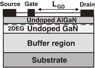
Most of the GaN power devices being developed adopt a lateral structure. In general, a device with a lateral structure is not suitable for high-power switching applications since the breakdown voltage is determined by the gate–drain distance LGD. In order to achieve a high breakdown voltage, LGD should be large, which results in a high on-resistance. However, the unique characteristics of GaN allow a low on-resistance to be achieved even at high voltage. The basic structure of a lateral GaN device is shown in Fig. 13, in which two-dimensional electron gas (2DEG) is formed at the AlGaN/GaN interface. The high-density 2DEG in the drift region results in a low-on-resistance device while maintaining a high breakdown voltage. A high breakdown voltage of 2.2 kV has been reported for the GaN heterojunction field effect transistor (HFET) on a Si substrate.28) However, the main target of the breakdown voltage for automotive applications is around 600 V because voltages of batteries used in HVs are 200–300 V. Moreover, the devices with a 600 V breakdown rating have a large market in consumer products. In general, it is difficult to achieve high current capacity in lateral devices because a large area of the chip is needed to accommodate large current. Therefore, a suitable electric power of the applications will be less than 10 kW.
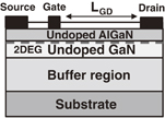
Fig. 13. Basic structure of lateral GaN power device. The breakdown voltage is determined by the gate-to-drain distance LGD.
Download figure:
Standard image High-resolution imageAnother unique property of the lateral GaN device is high-speed operation. The drift region consists of undoped AlGaN and GaN layers, which gives rise to a low feedback capacitance Cgd, making high-speed modulation possible. The low on-resistance and the feedback capacitance contribute to the high efficiency and compactness of power electronics modules. The characteristics of the lateral devices are suited to medium-power applications in HVs. Furthermore, the lateral device is also competent in the high-frequency amplifier of a wireless charging system of EVs as mentioned above.
A simple AlGaN/GaN structure was the basic layer structure, but recently, the structure has been improved to GaN/AlGaN/AlN/GaN. The top GaN layer (2–5 nm thick) reduces the density of surface states29,30) and is effective in suppressing current collapse, as will be discussed later. A thin AlN (1–2 nm thick) layer is inserted at the AlGaN/GaN interface. This improves the electron mobility in 2DEG because the AlN layer produces a high barrier, which reduces alloy scattering of electrons in an AlGaN layer. As a substrate for heteroepitaxy, a Si substrate is mainly used. Of course, a SiC substrate is a better choice for a power device because of its low thermal conductivity and high degree of lattice matching with GaN. However, the small size and high cost of SiC substrates restrict their adoption in commercial devices. Therefore, Si substrates are generally used in products. When the Si substrate is used, a buffer layer is essential to obtain a high-quality GaN layer. To guarantee a high breakdown voltage of over 600 V, the required thickness of the epitaxial layer is about 4 µm. The buffer layer relaxes the tensile stress in the epitaxial layer resulting from the difference in the thermal expansion coefficient between GaN and Si. Therefore, the buffer structure is the key to obtaining a high-quality epitaxial layer on Si. Individual epitaxial-wafer manufacturers have their own buffer structures that are based on AlN/GaN superlattices or pseudomorphic AlGaN layers. The present maximum diameter of the Si substrate is 150 mm, and an epitaxial growth technology on the 200 mm Si wafers is currently under development. The use of Si substrates and the fact that the fabrication process is similar to that for Si devices are very strong advantages for achieving high cost performance.
However, it is widely recognized that there are two serious issues with lateral GaN devices: current collapse and normally-off operation. These topics are discussed in the following subsections.
3.2.2. Current collapse
Current collapse refers to a reduction in the drain current during high-voltage switching. The current collapse must be suppressed in order to apply the GaN power device to high-voltage switching. This phenomenon is caused by negative fixed charges on the device surface31) and/or in the AlGaN and GaN layers.32,33) The negative charges reduce the 2DEG density in the drift region, which results in an increased on-resistance. The surface charges are redistributed from the gate owing to the high electric field concentration at the gate edge. The use of a field plate can alleviate such electric field crowding.34–37) An appropriate surface passivation film can also be employed to reduce the number of surface states that trap electrons.38) A combination of these methods is effective in suppressing current collapse. Another useful approach to reducing the number of surface states is to form a thin GaN cap above the AlGaN layer, as mentioned above.29) The cap has recently become popular when producing AlGaN/GaN on Si epitaxial wafers. Another related issue is the large number of dislocations and point defects in the epitaxial layers, some of which can trap negative charges. An electron trap in GaN bulk has been evaluated from the on-resistance transient after a long trap-filling pulse.39) The trap responsible for collapse had an activation energy of 1.03 eV, which is similar to that of a trap possibly related to dislocations.40) Therefore, improving the crystal quality is very effective in reducing the number of fixed charges in the AlGaN/GaN structure.41) The above measures allow current collapse to be suppressed for drain voltages of less than 600 V, and this was, therefore, the breakdown voltage quoted for the first commercial devices.2) However, a great deal of research is still being carried out for the complete elimination of current collapse.
3.2.3. Normally-off operation
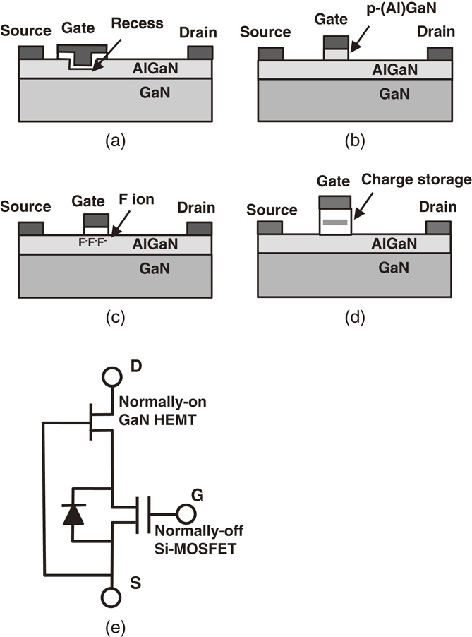
The second major issue with GaN power devices is achieving the normally-off operation, since this is made difficult by the high-density 2DEG at the AlGaN/GaN interface. In Si and SiC power devices, a MOS channel is usually used to obtain normally-off operation. An inversion gate forms a threshold voltage of over 3 V, which is generally required to prevent noise-induced errors in gate signal. Unfortunately, it is difficult to produce an inversion layer in GaN, and several alternative techniques for achieving normally-off operation have been proposed. These are summarized in Fig. 14.
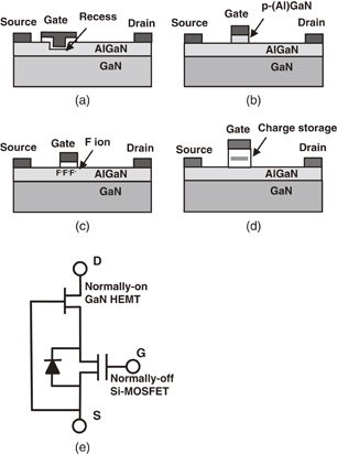
Fig. 14. Proposed normally-off gate structures. (a) Recess gate structure. (b) p-GaN or p-AlGaN gate structure. (c) Fluorine-ion-implanted structure. (d) Floating gate structure. (e) Cascode connection.
Download figure:
Standard image High-resolution imageThe proposed structure (a) in Fig. 14 involves a recessed-gate approach.42) The AlGaN barrier layer (∼20 nm thick) below the gate is etched to a thickness of 2–5 nm, which causes the 2DEG to almost vanish in this region,43) resulting in a positive shift in the threshold voltage. However, it is difficult to completely deplete the 2DEG to obtain a sufficiently high threshold voltage. If the recess is deep enough to penetrate the GaN layer, the 2DEG vanishes completely; this corresponds to a MOS gate structure. Normally-off operation was successfully achieved by this approach,44) even without the use of a p-type GaN layer. The weak points of such a MOS structure are a high channel resistance in the gate region and poor control of the threshold voltage.
The proposed structure (b) in Fig. 14 includes a p-GaN gate structure. This produces a depletion layer that extends from the p–n junction, thereby depleting the 2DEG, so that normally-off operation can be achieved.45,46) However, in this structure, the gate bias voltage higher than the built-in p–n potential leads to a large gate leakage current. This means that it is difficult to achieve a threshold voltage that is higher than the built-in p–n potential. On the other hand, a group at Panasonic has developed a new type of transistor using a p-AlGaN gate, named the gate injection transistor (GIT).45) They exploited the hole injection from the p-AlGaN gate to the channel, which resulted in low on-resistance owing to the conductivity modulation. In the fabrication of this type of device, the selective removal of the p-(Al)GaN layer is difficult. Dry etching control to stop the etching at the AlGaN barrier layer and the reduction of etching damage on the etched surface will be issues to be investigated.
The third approach (c) in Fig. 14 involves fluorine ion implantation into the AlGaN layer in the gate region. The negatively charged ions effectively deplete the 2DEG electron; thus normally-off operation is achieved.47) One technical difficulty is ensuring that no fluorine ions penetrate the GaN layer. If this occurs, the channel mobility deteriorates markedly.
The fourth structure (d) in Fig. 14 is a floating gate structure similar to that of flash memory.48) The gate structure consists of a tunnel dielectric layer, a charge storage layer, and a blocking dielectric layer. Electrons are injected to the charge storage layer through the tunnel dielectric layer by the large positive bias of the control gate. The threshold voltage of the device is defined by the number of charged electrons. High performance of the floating gate had been predicted.49) However, the main problem of the floating gate structure is short retention time.
Although normally-off operation has been realized with all of the above structures, the gate voltages of the structures in the subthreshold range are around 1 V, which is lower than that for a conventional Si-MOSFET. Therefore, to achieve stable and reliable operation, a gate drive circuit that is suitable for low-threshold-voltage devices must be developed.
The final structure (e) for normally-off operation illustrated in Fig. 14 is a cascode connection using a high-voltage normally-on GaN HFET and a low-voltage normally-off Si-MOSFET.50) In this configuration, the source of the Si-MOSFET is connected to the gate of the GaN HFET. Thereby, the gate–source voltage VGS for the GaN HFET has an opposite sign to the drain–source voltage VDS for the Si MOSFET. When the Si MOSFET switches off and the voltage across the device rises, this voltage switches off the GaN HFET. Conversely, when the Si-MOSFET switches on, the GaN HFET switches on as a response to VDS for the Si-MOSFET dropping to a very low value. These two devices can be encapsulated in a single package to produce a three-terminal device. Since the threshold voltage is determined by the Si-MOSFET, this enables high threshold voltages (>3 V). This configuration is a realistic solution to the high threshold requirement. Although the on-resistance was the sum of the on-resistances of the two devices, high performance of the cascade GaN HFET was achieved.51)
3.2.4. Advanced research
Although the AlGaN/GaN heterostructure has a long history and is a proven technology, other heterostructures or gate structures for improving the device performance are being developed. In this subsection, these advanced approaches are described.
An AlN/GaN insulated-gate HFET was first reported in 1998 by a group from Sony.52) The lattice mismatch between AlN and GaN is about 2.5%, which results in the production of a large number of strain-induced piezoelectric charges and spontaneous polarization charges at the AlN/GaN interface. Under recent optimized growth conditions for the AlN layer, a high 2DEG density (∼2.7 × 1013 cm−2) and a high mobility (∼1400 cm2·V−1·s−1) have been obtained. The AlN/GaN heterostructure resulted in a very low sheet resistance of ∼165 Ω/sq and the AlN/GaN HFET showed a high current density of 2.3 A/mm.53) This heterostructure has mainly been applied to high-frequency devices.53,54) A lattice-matched InAlN/GaN heterostructure was first proposed by Kuzmik.55) For InAlN with a 17% In content, the lattice constant is the same as that of GaN. In such an InAlN/GaN heterostructure, no stress is generated, in contrast to the case of an AlGaN/GaN heterostructure. The lack of stress leads to high reliability. Moreover, InAlN has a large spontaneous polarization that produces a high 2DEG density. High-performance, high-frequency devices based on the InAlN/GaN structure have been reported.56) Although the two types of heterostructures discussed above exhibit very good performance when used in high-frequency devices, it is not clear whether they can be applied to high-power switching devices because there is little data on high-voltage switching.
A new concept of the gate channel has been developed, and is named the multi mesa-channel (MMC) high-electron mobility transistor (HEMT).57) Very narrow mesas with top widths <100 nm are fabricated under the gate electrode. Threshold shift in the positive direction, small subthreshold slope, and current stability under high drain voltage stress have been observed. Similar gate structures have also been investigated. Normally-off operation with high drain current58) and suppression of the short channel effect59) have been observed.
A unique advantage of the lateral GaN device is the ease of integration. A monolithic three-phase inverter IC using GITs and the demonstration of motor drive have been reported.60) Research on power IC technology based on GaN devices has been proposed.61) The monolithic integration of lateral devices will become a key technology in the near future.
4. Reliability
Reliability is essential for realizing practical applications of new power devices. Reliability can be divided into short- and long-term components. Short-term reliability is related to the sudden death of a device, whereas long-term reliability corresponds to the device lifetime. The main indicators used to evaluate reliability are avalanche ruggedness, short-circuit capability, electrostatic breakdown, and gate insulator deterioration. The first three are related to the sudden death of a device.
For GaN power devices, avalanche ruggedness is the main issue. Avalanche breakdown is caused by a high-voltage surge due to a counter-electromotive force in an inductive load. In power applications, there are many inductive loads, such as motors. Si power devices maintain sufficient avalanche ruggedness for the high voltage surge by adopting an effective devices structure. However, in many cases, GaN HFETs are destroyed catastrophically when breakdowns occur. For a Schottky gate lateral GaN HFET, gate leakage caused by dislocations gives rise to a current concentration at the leakage point under the high-voltage surge, and it induces thermal destruction of the device. Therefore, the Schottky gate structure is not suitable for high-voltage applications since the heteroepitaxial layer used in a lateral device contains many threading dislocations. The metal–insulator–semiconductor (MIS) gate structure is effective for suppressing the gate leakage current. Normally-off devices need the MIS gate structure since positive gate bias has to be applied. However, the MIS gate GaN HFET is also catastrophically destroyed under high drain voltage because it has no effective structure against high-voltage surge. A p-type region inserted near the channel is effective for obtaining the avalanche ruggedness because the p-type region drains holes made by avalanche breakdown. Figure 15(a) shows simulation results of drain current under a drain voltage varying from 0 to 400 V in the off state for the MIS GaN HFET without and with a p-GaN region. The simulated device was a recessed gate normally-off GaN HFET with an Al2O3 insulated gate film. The p-type GaN region is inserted beneath the source to the source-side gate edge. The device without the p-GaN region turns on at 300 V. The simulation revealed that the impact ionization occurred at the drain-side gate edge and the holes began to accumulate under the gate as shown in Fig. 15(b), because there was no p-type region in the device structure. The accumulated holes turn on the device and pull electrons into the channel, generating additional holes by impact ionization. This cycle induces a large drain current and catastrophic thermal destruction occurs. On the other hand, the device with the p-GaN region shows no destruction because of little hole accumulation, as shown in Fig. 15(c). These simulation results indicate that a low-resistance p-type region is needed in order to remove the holes generated by the avalanche event. However, p-type doping is a weak point for GaN and related materials. The suitable p-type dopant is only Mg at the present time. However, the acceptor level of Mg is deep and Mg atoms easily diffuse in the GaN crystal. These characteristics of p-GaN make the formation of a low-resistivity and stable p-type region difficult. Therefore, a new effective approach to producing a p-type GaN region is strongly required in order to achieve high avalanche ruggedness.

Fig. 15. (a) Simulation results of off-state drain current of MIS GaN HFET with and without p-type region. (b) Hole concentration for the device without p-type region. (c) Hole concentration for the device with p-type region.
Download figure:
Standard image High-resolution imageThe MIS structure used in the lateral GaN HHET has a noteworthy subject. That is, dielectric breakdown takes place first in the device structure in many cases. This is due to the high critical electric field of AlGaN, which is of the same order of magnitude as that of gate insulator materials. Figure 16(a) shows the simulated electric field distribution for a simple MIS gate model. The gate insulator is SiO2 (thickness = 50 nm, ε = 3.9). Figure 16(b) shows the electric field under the gate edge for a drain bias varying from 100 to 1200 V.62) For a drain bias of 600 V, the electric field in the SiO2 film is 8 MV/cm, which is near the breakdown field of SiO2. At the same drain bias voltage, the field strength in AlGaN is less than the AlGaN breakdown field of 3 MV/cm. Thus, these results indicate that the SiO2 will break first. Therefore, in order to ensure that avalanche breakdown occurs in the semiconductor layer, a suitable device design to reduce the electric field in the insulator film is very important.
Download figure:
Standard image High-resolution image
Fig. 16. (a) Simulated electric field distribution in AlGaN/GaN HFET. (b) Electric field in SiO2 and at AlGaN/GaN interface.
Download figure:
Standard image High-resolution imageAs mentioned above, preventing the catastrophic death of lateral GaN power devices is difficult at the present time. Therefore, to guarantee reliability, the real breakdown voltage of the device should be substantially higher than the maximum rated voltage. Protection measures, such as the inclusion of snubber circuits or Zener diodes for absorbing current surges, are also effective.
Another important reliability issue is the lifetime of the gate insulator. The gate insulator is constantly exposed to gate bias stress, which can induce defects in the film. Therefore, the lifetime of the gate insulator limits the device lifetime. Evaluation of the insulator film is usually carried out by time-dependent dielectric breakdown (TDDB) measurements. Examples of breakdown and TDDB characteristics for an Al2O3 film on GaN deposited by atomic layer deposition (ALD) are shown in Figs. 17(a) and 17(b), respectively. The calculated Fowler–Nordheim (FN) current through Al2O3 film on GaN is also shown in Fig. 17(a). The discrepancy between the observed current and the ideal FN current suggests that the ALD Al2O3 film contains many defects and impurities that induce leakage current and electron traps. The FN current appears from ∼3 MV/cm. This indicates that the electric field in the gate insulator must be lower than 3 MV/cm under normal operation conditions because the leakage current reduces the lifetime of the insulator. The TDDB characteristics of the Al2O3 film at room temperature (RT), 150 °C, and 250 °C are shown in Fig. 17(b). Power devices for automotive applications require a TDDB lifetime of more than 20 years. For an electric field of 3 MV/cm, it can be seen that the lifetimes at RT and 150 °C satisfy this criterion, but that at 250 °C does not. For the GaN power devices, operation temperatures exceeding 200 °C are expected in the automotive applications. Thus, it is necessary to improve the high-temperature TDDB characteristics of this Al2O3 film. Many types of films are being evaluated for use as gate insulators. These candidate films should be examined from the viewpoint of not only their interface state density and breakdown voltage but also their lifetime.

Download figure:
Standard image High-resolution image
Fig. 17. (a) Breakdown characteristics of ALD Al2O3 film on GaN. (b) TDDB lifetime measurement of ALD Al2O3 film.
Download figure:
Standard image High-resolution image
The reliability of the devices is a neglected but indispensable issue to conquer the valley of device death. Identifying the issues related to reliability will yield a shorter path to practical applications.
5. Conclusions
The performance of the GaN power device is highly suitable for automotive applications. Lateral GaN power devices are expected to exhibit excellent performance in medium range power modules in HV and EV systems. Vertical GaN power devices will also become key devices for high-power modules if the potential can be drawn out. Since two major issues of the lateral GaN device, current collapse and normally-off operation, are being improved, the lateral devices are now approaching practical use. On the other hand, progress of the vertical GaN devices is slower than that of the lateral devices. Many issues in the development of the vertical GaN devices still remain unresolved. However, the GaN substrate quality has recently been improved to the level of being applicable to high-voltage vertical GaN devices. The development environment is continuously being upgraded.
Biographies

Tetsu Kachi received the B.E., M.E., and Ph. D. degrees in applied physics from Nagoya University in 1975, 1977, and 1985, respectively. He joined Toyota Central R&D Labs., Inc. in 1978. His researches in the laboratory were optical measuring system, GaAs laser, GaN laser and GaN LED developments. Since 2000, his main interest has been GaN power devices. He served as chair of the Electron Devices (ED) Technical Committee of IEICE from 2011 to 2012. He is now a Fellow of Toyota Central R&D Labs., Inc.