
Abstract
One of the key problems in the synthesis of group III nitrides is the development of an effective source of reactive nitrogen, which is necessary for incorporation into the crystal lattice. In this paper, we describe a source of reactive nitrogen based on ECR discharge plasma, which is sustained by technological gyrotron radiation. Measurements of atomic nitrogen flux were conducted by mass-spectrometric analysis of the products of the reaction of nitrogen monoxide with atomic nitrogen. The maximal atomic nitrogen flow was 5 × 10¹⁸ atoms/s (12 sccm). The atomic source was used to grow InN films.
Export citation and abstract BibTeX RIS
In recent years, A3B5 compounds have become very popular owing to their unique and promising properties. Heteroepitaxial films of these compound semiconductors have attracted great interest from researchers because of the possibility of using them for effective optoelectronic devices and microwave electronic devices.1–4) The most challenging among these compounds is indium nitride. The predicted properties of this material are extremely tempting;5) however, it is still difficult to realize them in practice. Since growing indium nitride from the melt is impossible,6) the only way to grow InN is layer-by-layer deposition.
The best heteroepitaxial layers can be obtained by the plasma-assisted molecular beam epitaxy (PA MBE) method. However, in this method also, it is necessary to conduct crystal growth at temperatures insufficient for high-quality growth. The main restriction is the decomposition of indium nitride at high temperatures.7) Increasing the growth temperature leads to an enhanced degradation of the material, which consequently requires an increase in the flow of reactants, particularly, active nitrogen. It was shown that increasing the flow of reactive nitrogen makes it possible to grow InGaN films at higher temperatures, resulting in a better crystalline quality.8) Indeed, from the data presented in Ref. 9, one can find that for InN growth at 700 °C it is necessary to provide at least 1017 cm−2 s−1 of active nitrogen flux to compensate for material decomposition. In this paper, we propose a new source of atomic nitrogen based on the plasma of electron cyclotron resonance (ECR) discharge, which is sustained by microwave radiation at a frequency of 24 GHz for the growth of InN and InGaN with high indium contents.
Nitrogen activation in plasma has obvious advantages. In nitrogen-activation-based methods, the rate of active nitrogen supply in the growth zone is determined by plasma parameters and is independent of substrate temperature (in contrast to NH3-based methods). The use of a technological gyrotron as a source of microwave radiation, with high frequency and power provides additional capacity to adjust the flux of activated nitrogen. This gives grounds to expect a significant increase in active nitrogen flux. We propose the use of the ECR discharge produced and sustained by CW gyrotron radiation with powers up to 5 kW and a frequency of 24 GHz for the growth of heteroepitaxial indium nitride films and InGaN films with high In contents. Heating at a high (compared with the conventional source: magnetron 2.45 GHz) frequency can significantly increase the plasma density in the discharge, which provides an increased rate of molecular nitrogen dissociation (excitation). In addition, a high average power of gyrotron radiation provides a high specific power absorbed in the plasma,10) which can be up to 100 W cm−3.
The scheme of the setup is presented in Fig. 1. The microwave radiation (1) of the technological gyrotron (2) is injected into the plasma chamber (3) through the window. The magnetic coil (4) provides the conditions for ECR discharge. Molecular nitrogen (5) goes to the plasma discharge zone, where it is dissociated upon electron impact. After exiting the reactor, the flow of activated nitrogen enters the growth chamber, where the substrate is placed on a heated substrate holder (6). Trimethylindium is injected near the substrate (7). Thermal decomposition of trimethylindium on the substrate surface in a stream of active nitrogen provides the indium nitride film growth. Langmuir probes were placed at the center of the reactor at the position of the substrate holder to measure plasma density. A gas line (7) was used for NO supply for atomic flux measurements.

Fig. 1. Setup scheme. 1: microwave radiation, 2: gyrotron, 3: nitrogen plasma, 4: magnetic coil, 5: nitrogen supply line, 6: substrate holder, 7: trimethylindium or NO supply line, 8: pumping port.
Download figure:
Standard image High-resolution imageAt the very beginning of investigations, our challenge was to determine the range of driving parameters, wherein the ECR discharge exists, and also to measure the major properties of plasma. The goal of our study was to clarify the optimum conditions for discharge ignition; in particular, to design the best geometry of the vacuum chamber, wherein the maximum density and temperature of plasma electrons — the key factors affecting the rate of plasma-chemical reactions, can be obtained. The experiments on the setup with continuous ECR discharge were carried out using nitrogen as the working gas. Preliminary experiments were conducted in the vacuum chamber, which includes the plasma chamber and reactor. The investigations showed that in the present configuration of the vacuum chamber the steady state of discharge exists while the magnetic field exceeds a resonance value of 0.86 T and the gas pressure is higher than 1.2 × 10⁻² mbar. The breakdown pressure threshold of the gas hardly depends on microwave power. The minimum power necessary for discharge ignition is 300 W.
To measure plasma parameters, we used the double-probe Langmuir probe placed along the system's axis in the reactor part of the vacuum chamber 26 cm from the center of the discharge. We suppose that the plasma spreads along the magnetic field lines, which is why the plasma density at the maximum magnetic field (B ∼ 10000 G) exceeds approximately one thousand times the density measured by the probe (B ∼ 10 G). Note that in the following results, the plasma density and temperature presented here correspond to the maximum magnetic field at the center of discharge. Figures 2 and 3 show the results of measurements of electron density and temperature as a function of microwave heating power at a gas pressure of 2 × 10⁻² mbar. It is clearly seen from the figures that the plasma density and temperature increase with increasing applied microwave power. Under such conditions of experiments the plasma density and temperature reach the maxima of 1.5 × 1011 cm−3 and 4 eV, respectively, at a power of ∼900 W. The essential success in advancing into the highest plasma density was achieved by modifying the configuration of the vacuum chamber — the outlet of the plasma reactor was closed by the grid. The grid was transparent for the plasma and atomic nitrogen flow, but the microwave field was trapped inside the plasma chamber. It is clear that the resulting cavity greatly increases the electric field strength and enhances the effectiveness of energy transmission from the microwave radiation to electrons. In this new configuration the discharge exists under the same conditions as in the previous configuration. However, a stable gas breakdown occurs at an essentially low gas pressure of ∼8 × 10⁻⁵ mbar, which results in a sufficiently increased plasma ionization degree. Thus, at a gas pressure of ∼2 × 10⁻² mbar and a microwave power of ∼400 W, the electron density is about ∼3 × 1011 cm−3 and the electron temperature is about 4 eV, which are several times higher than those obtained in the previous experiments. Figures 2 and 3 show the results of measurements of electron density and temperature as a function of microwave heating power at the gas pressure of 2 × 10⁻⁴ mbar. It is clearly seen from the figures that in the low-pressure range one can obtain a plasma density more than one order of magnitude higher than that under the previous conditions. The maximum electron density of ∼3 × 1012 cm−3 is achieved at the gas pressure of ∼2 × 10⁻⁴ mbar and power of ∼1100 W. The electron temperature is about 5.3 eV. Note that in this case, the plasma ionization degree becomes very significant and can reach 20–40%.

Fig. 2. Electron temperature as a function of heating microwave power at two different pressures of nitrogen as a working gas.
Download figure:
Standard image High-resolution image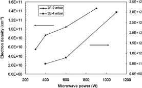
Fig. 3. Plasma density as a function of heating microwave power at two different pressures of nitrogen as a working gas.
Download figure:
Standard image High-resolution imageMeasurements of atomic nitrogen flux of the ECR plasma discharge were carried out by titration reaction.11,12) The method consists of carrying out the reduction reaction of nitrogen monoxide (NO), which is added at a known amount. Atomic nitrogen restores the monoxide by the following reaction: N + NO → N2 + O. Nitrogen monoxide was supplied through a tube of stainless steel, whose outlet was at the center of the atomic nitrogen flux and was directed downstream of the gas flowing from the plasma chamber (see Fig. 1). The gas mixture containing 10% NO and 90% N2 was used in the experiments. To analyze the composition of the mixture of reacting gases in an exhaust outlet after the turbo pump and before the inlet of the fore vacuum pump, a specimen was taken. Subsequent analysis of the specimen was performed by quadrupole mass-spectrometry. The dependences of nitrogen atomic flux on microwave power and molecular nitrogen flow are shown in Figs. 4 and 5, respectively. The dependence of atomic nitrogen flux on microwave power exhibits saturation, which is achieved at 500 W and a molecular nitrogen flow of 730 sccm. The dependence of atomic nitrogen flow on input power indicates that the electron temperatures of 1.6–1.8 eV are sufficient for the effective excitation of rotational and vibrational degrees of freedom13) of the N2 molecule. Starting from these values, a significant fraction of the energy deposited in the discharge goes into gas heating by the excitation of rotational and vibrational degrees of freedom and the following collisions. Hot gas reduces the concentration of molecules at a fixed flow, which leads to a decrease in the rate of dissociation of the molecules. The dependence of atomic nitrogen flux on N2 flux through the source is almost linear in the saturation region of power. The linear dependence of atomic nitrogen flux on the total gas flow through the plasma is further indicative of the heating and expansion of the gas in this mode. Consequently, greater gas flow through the plasma prevents the heating of the gas, thereby increasing the efficiency of dissociation. The maximum atomic nitrogen flux of 5.4 × 10¹⁸ atoms/s is achieved at a higher heating power of 950 W (see Fig. 5). Thus, the source of atomic nitrogen with a performance of 5 × 10¹⁸ atoms/s or 12 sccm is demonstrated. This record value of atomic nitrogen flux was realized at a molecular nitrogen flow of 1150 sccm and a microwave power of 950 W. The ionization degree was about 0.5%, while the neutral gas pressure in the analysis chamber was 0.1 mbar.
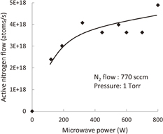
Fig. 4. Active nitrogen flux vs microwave power.
Download figure:
Standard image High-resolution image
Fig. 5. Active nitrogen flux vs N2 flux through the source.
Download figure:
Standard image High-resolution imageTo determine the prospects of such a source of nitrogen indium nitride layers on different substrates, growth experiments were conducted.14,15) The possibility of low-temperature growth of a monocrystalline InN layer was demonstrated in Ref. 14. InN film growth was performed under the following conditions: heater temperature, 360 °C; nitrogen flow through the plasma reactor, 91 sccm; nitrogen flow through trimethylindium in the bubbler, 23 sccm; pressure in the growth chamber, 0.37 mbar; and microwave power, 550 W. InN films grown on different substrates have a uniform mirror-like smooth surface. Scanning electron microscopy (SEM) investigations showed that the InN films grown on yttria-stabilized zirconia (YSZ) (111) substrates have a grain structure with a grain diameter in the range of 50–150 nm. Epitaxial InN films grown on templates have a uniform surface with a wavy relief and no grain structure, the same as the template. The surface roughness values of the InN films grown on YSZ (100) and YSZ (111) with 0.8 µm thickness are, respectively, 2.5 and 1.6 nm rms. The surface roughness of InN films grown on templates was slightly higher (6 nm rms) than the films grown on YSZ substrates. This is probably related to the roughness of the template used (5 nm rms). No indium droplets were found on the surface of InN films. Figure 6 shows the X-ray diffraction (XRD) spectrum in the φ scanning mode of the InN film grown on Al2O3 (0001) with a double buffer layer (template). There are sharp peaks that run through 60°, indicating a single-crystal structure of the film. The minimum half-width of the rocking curve peak InN (0002) is 0.3°. The XRD spectrum in the (2θ–ω) scanning mode shows only line series (000l) for the InN phase, and the line's intensity is higher than that in the original InN buffer layer. The In phase is not observed. The photoluminescence (PL) spectrum of InN films grown on a template (InN/GaN/Al2O3) is shown in Fig. 7. The PL spectra of the InN film representing the top layer of a double buffer layer and of the InN film grown on the YSZ substrate are also shown in Fig. 7. It is clearly seen that the InN films grown on the YSZ substrate and template have intense room-temperature PL in the infrared region (1490–1540 nm). These results prove that it is possible to grow monocrystaline InN films with good optical properties at a relatively low temperature (360 °C).
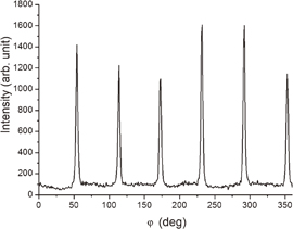
Fig. 6. XRD spectrum (φ scan) of InN film grown on Al2O3 (0001) substrate with InN/GaN double buffer layer.
Download figure:
Standard image High-resolution image
Fig. 7. PL spectra: (1) template, (2) InN film grown on YSZ (100), and (3) InN grown on template.
Download figure:
Standard image High-resolution imageIn Ref. 15, it was aimed to demonstrate the rapid growth of indium nitride layers while maintaining single crystals at an acceptable level. InN hexagonal monocrystalline films were grown on YSZ (111) and Al2O3 (0001) by the organometallic vapor phase epitaxy method with nitrogen activation in the ECR discharge, supported by gyrotron radiation. The film growth rate reached 10 µm h−1. Figures 8 and 9 show the XRD spectra (ω-scan) and PL spectra of InN films with different substrates. The results reported in Ref. 15 can be summarized as follows: (1) The active nitrogen source based on the ECR discharge sustained by the gyrotron radiation makes it possible to produce InN films of high quality at growth rates up to 10 µm h−1. (2) The use of cubic zirconia substrates (111) compared with sapphire substrates (0001) and the template GaN/Al2O3 (0001) can significantly improve the structural quality of the films of InN. InN films grown on YSZ (111) have a minimum width of the XRD rocking curve of 930 arcsec. The RMS surface roughness in this case was only 1.25 nm. (3) InN films grown on YSZ (111) and template GaN/Al2O3 have an intense PL in the infrared region.

Fig. 8. XRD spectra (ω-scan) of InN films with different substrates. 1: Al2O3 (0001), 2: GaN/Al2O3 (0001), 3: YSZ (111).
Download figure:
Standard image High-resolution image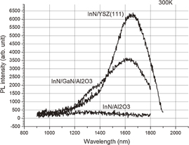
Fig. 9. PL spectra of InN films with different substrates at room temperature. 1: Al2O3 (0001), 2: GaN/Al2O3 (0001), 3: YSZ (111).
Download figure:
Standard image High-resolution image
The measured flux of atomic nitrogen and the high-speed deposition of epitaxial layers of indium nitride, which confirm the high flux of atomic nitrogen from the source described, open up new prospects for improving the quality of indium nitride films. The key parameter determining the structural perfection of epitaxial layers of InN is the growth temperature of a layer. The performance of the atomic nitrogen source allows the increase in the growth temperature and the compensation for the increased rate of nitrogen escape from the film, maintaining the stoichiometric ratio of indium to nitrogen.7)
In conclusion, a new source of atomic nitrogen based on the plasma of the ECR discharge, which is sustained by microwave radiation at a frequency of 24 GHz for the growth of InN and InGaN with a high indium content, is proposed. The maximum performance of the atomic nitrogen source is 5 × 10¹⁸ atom/s. This amount of atomic nitrogen flow enables the growth of indium nitride at previously inaccessible temperatures, offsetting the high rate of decomposition of indium nitride.
Acknowledgments
The authors are very grateful to Professors Sergey Ivanov and Professor Sergey Golubev for fruitful discussions. The work was supported by the Russian Foundation for Basic Research; Grant No. 13-02-97087, Russian Academy of Sciences (Program of Presidium No. 1).