Abstract
Potential-induced degradation (PID) of Cu(In,Ga)Se2 (CIGS) photovoltaic (PV) modules fabricated from integrated submodules is investigated. PID tests were performed by applying a voltage of −1000 V to connected submodule interconnector ribbons at 85 °C. The normalized energy conversion efficiency of a standard module decreases to 0.2 after the PID test for 14 days. This reveals that CIGS modules suffer PID under this experimental condition. In contrast, a module with non-alkali glass shows no degradation, which implies that the degradation occurs owing to alkali metal ions, e.g., Na+, migrating from the cover glass. The results of dynamic secondary ion mass spectrometry show Na accumulation in the n-ZnO transparent conductive oxide layer of the degraded module. A CIGS PV module with an ionomer (IO) encapsulant instead of a copolymer of ethylene and vinyl acetate shows no degradation. This reveals that the IO encapsulant can prevent PID of CIGS modules. A degraded module can recover from its performance losses by applying +1000 V to connected submodule interconnector ribbons from an Al plate placed on the test module.
Export citation and abstract BibTeX RIS
1. Introduction
Very large-scale photovoltaic (PV) systems, which can generate a high electric power, have been installed worldwide over the last decade. The PV modules in such systems can be exposed to high electrical potential differences from their grounded frames. These may trigger potential-induced degradation (PID), which may cause significant performance losses of the modules.1–3)
PID of p-type crystalline Si (c-Si) modules is characterized by a reduction in the shunt resistance Rsh1) and enhancement of depletion region recombination.4,5) PID of p-type c-Si PV modules can be attributed to alkali metal ions, e.g., Na+, migrating from the module cover glass owing to high voltages.3) Naumann et al.6) have revealed that Na accumulates into the SiNx/Si interface in PID-affected regions. It has been reported that both PID shunts and Na accumulation are constrained to local spots.7,8) Moreover, it has been implied that stacking faults existing in Si contaminated by Na play an important role in PID.8) Some researchers have proposed physical models that can explain the shunting mechanisms6,7,9,10) and enhanced depletion region recombination.10,11)
PID of c-Si PV modules is affected by module components, such as the cover glass, encapsulant, and cells. It has been demonstrated that modules with a quartz cover glass show no significant PID.4) PID can be prevented by using a high-electrical-resistance encapsulant instead of an ethylene-vinyl acetate copolymer (EVA)4,12) and by inserting a polyethylene film with a thickness of 30 µm between the cover glass and the EVA encapulant.13) PID resistance is also affected by the refractive index2,14,15) and the thickness2) of the SiNx antireflective coating (ARC) layer on the emitter layer of c-Si PV cells. PID can therefore also be suppressed by controlling the composition of the ARC layers. However, it is not very desirable that the refractive index is changed from conventional and optimized values. Mishina et al.16) have shown that PV cells with an ARC layer prepared by plasma-enhanced chemical vapor deposition using a hollow cathode have a high PID resistance with a maintained conventional refractive index. The coauthors17) have reported that TiO2 thin films deposited on the inner surfaces of the cover glass can prevent PID of c-Si modules. PID-affected modules can recover from the degradation by applying a positive bias.1,18) The recovery is explained as a diffusion-driven process.9,10,19)
The degradation mechanism in thin-film Si PV modules differs from that in c-Si PV modules.20) Hence, PV modules consisting of other cell materials may degrade by different mechanisms. Very few research papers on PID have, however, been published except for PID of c-Si systems.
Cu(In,Ga)Se2 (CIGS) thin-film PV modules, as shown in Figs. 1 and 2 described in Sect. 2.1 have attracted attention because of their cost-effectiveness and high energy conversion efficiency. Recently, Powalla et al.21) have reported the highest efficiency of 21.7% for a small-area cell of Al-doped ZnO/i-ZnO/CdS/CIGS/Mo/glass substrate. In addition, CIGS PV modules show no light-induced degradation, which may lead to better long-term stability than thin-film amorphous Si (a-Si) modules. For these reasons, CIGS PV modules have started to be installed in very large-scale PV systems. Knowledge of PID is not, however, sufficient to stably operate PV systems consisting of CIGS modules.

Download figure:
Standard image High-resolution image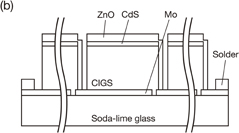
Fig. 1. Schematic diagrams of (a) single cell and (b) integrated submodule. The CIGS integrated submodule is composed of 17 cells with an area of about 80 × 4.8 mm2 connected in series. Refer to the report by coauthors24,25) for information on details of submodule fabrication.
Download figure:
Standard image High-resolution image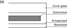
Download figure:
Standard image High-resolution image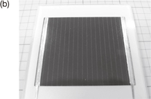
Fig. 2. (a) Schematic diagram of structure of modules and (b) appearance of a CIGS module. The sizes of the submodules and modules are 80 × 80 and 120 × 120 mm2, respectively. The vertical stripes are the individual cells with a width of 4.8 mm. Interconnector ribbons are placed on the both sides of submodule.
Download figure:
Standard image High-resolution imageTypical CIGS PV cells shown in Fig. 1 have soda-lime glass (SLG) substrates containing Na. Na is naturally introduced into their CIGS light-absorbing layers from glass substrates during deposition, which can lead to a higher energy conversion efficiency.22) Fjällström et al.23) have, however, reported that CIGS PV cells suffer from PID due to Na migrating from their glass substrate during PID stressing. They have also revealed that a degraded cell with an SLG substrate shows an increased Na concentration in a CdS layer and the upper region of a CIGS layer. These indicate that PID of CIGS cells may be caused by Na. Fjällström et al. have provided an important hint on PID of CIGS PV. On the other hand, their PID experiment was far from real PID observed outdoors, since they used not modules but small-area cells. For standard CIGS modules, Na exists in the cover glass, as well as glass substrates and CIGS light-absorbing layers, which may also degrade CIGS modules. PID of laminated CIGS modules has not, however, been reported in detail so far.
PID acceleration tests have been used in order to easily obtain degraded modules in a short time. The tests of modules are conducted by applying a voltage bias to cells (1) from the grounded Al frame of modules flooded with water on their cover glass side,1) (2) from the grounded Al frames in damp heat,3) or (3) from an Al plate placed onto their cover glass in dry environment.17) In this work, we used the third way in order to obtain degraded samples. Note that this acceleration test is severe; in particular, modules fabricated from multicrystalline Si and thin-film a-Si cells show total failure after the test for 2 h and 3 days, respectively, which will be shown in Sect. 3.4.
In this work, using the PID acceleration test, PID of CIGS modules fabricated from integrated submodules was studied. Then, we used test modules fabricated from several different components to investigate the effect of module components on degradation behavior. Diffusion behavior of Na was investigated by dynamic secondary ion mass spectrometry (D-SIMS). In addition, by comparing PID test results of CIGS modules with those of PID-prone multicrystalline Si modules and a standard thin-film a-Si module, we discuss the PID resistance of CIGS modules.
2. Experimental procedure
2.1. Fabrication of submodules and modules
The structure of individual cells and the integrated submodule are shown in Fig. 1. A single cell is composed of n-ZnO:Al/ZnO/CdS/CIGS/Mo/soda-lime glass and has no surface texture or ARC layer. The integrated submodule contains 17 cells connected in series. Individual single cells are separated by scribing lines as indicated in Fig. 1(b). Refer to reports by the coauthors24,25) for detailed information on submodule fabrication.
The structure of modules and the typical appearance of a CIGS module are shown in Fig. 2. As illustrated in Fig. 2(a), stacking structures composed of cover glass/encapsulant/CIGS submodule/encapsulant/typical backsheet [poly(vinyl fluoride) (PVF)/poly(ethylene terephthalate) (PET)/PVF] were prepared. CIGS PV modules were fabricated from the stacking structures with a module laminator. Our lamination process was composed of two stages: the degassing stage for 5 min and the adhesion stage for 15 min. The stacking structures were placed with the cover glass side down on the heater maintained at 135 °C during lamination. A non-alkali glass as the cover glass as well as a conventional tempered glass was used in order to understand the effect of alkali metals in cover glass on degradation. Conventional tempered glass contains Na, whereas non-alkali glass contains no Na. Ionomer (IO; Tamapoly HM-52) as well as EVA was also used as encapsulant materials in order to investigate the effect of encapsulants on degradation. It is known that IO encapsulants have high resistivity. We name these samples to classify those having different components, and list these names in Table I. Samples will be referred to as "Sample A" for the sample containing the tempered glass and EVA encapsulant, "Sample B" for the sample containing the non-alkali glass and EVA encapsulant, and "Sample C" for the sample containing the tempered glass and IO encapsulant.
Table I. Names of the CIGS module samples.
| Sample name | Cover glass | Encapsulant |
|---|---|---|
| Sample A | Tempered | EVA |
| Sample B | Non-alkali | EVA |
| Sample C | Tempered | IO |
2.2. PID tests and characterization
The PID tests were performed by applying a voltage of −1000 V to connected submodule interconnector ribbons from an Al plate placed on test modules at 85 °C. We use the term "PID stress" here to refer to such voltage and temperature stress. The measured relative humidity was approximately 2% in a chamber for our PID tests. At a high humidity, for example 85%, moisture ingress into PV modules induces the electrical corrosion of transparent conductive oxide (TCO) layers.20) The humidity in our setup was much lower; thus, we neglected the influence of humidity under this experimental condition. (Actually, delamination as a consequence of electrical corrosion of TCO layers did not occur after any PID tests.) We also applied +1000 V to the connected submodule interconnector ribbons of the degraded sample in order to investigate the effect of the positive bias applied to CIGS modules. The PID tests of multicrystalline Si and a-Si PV modules were also carried out for comparison.
In order to evaluate the degradation, illuminated and dark current–voltage (I–V) measurements were conducted for modules before and after each PID test. Electroluminescence (EL) images were recorded at a current density of about 25 mA/cm2 in order to visualize degradation positions. The current density for EL measurement was set to obtain strong luminescence from unaffected CIGS modules. We carried out D-SIMS measurements using a CAMECA IMS-6f apparatus with a Cs+ primary ion beam in order to obtain elemental depth profiles of samples.
3. Results and discussion
3.1. Degradation behavior in CIGS modules
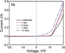
We show the dependence of the I–V curves under illumination of Sample A (with the conventional tempered glass and EVA encapsulant) on PID-stress duration in Fig. 3. The I–V curves change substantially as the durations of PID stress increases, and then the normalized energy conversion efficiency to the initial value η/η0 of Sample A decreases to about 0.2 after the PID test for 14 days. Another module, with the same composition as Sample A, heated at 85 °C for 14 days without PID stress did not show significant performance loss, as shown in Fig. 4. These results reveal that CIGS modules suffer from PID under this experimental condition. As can be seen in Fig. 3, it is observed that both the open circuit voltage Voc and the fill factor FF drastically decrease after PID stress for 14 days. In contrast, the short circuit current Isc remains almost constant until the PID-stress duration reaches 7 days and slightly decreases after PID stress for 14 days. The degradation is therefore characterized by reductions in Voc and FF.
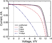
Fig. 3. Dependence of the I–V characteristics of Sample A under illumination on the PID-stress duration. The PID tests were performed by applying −1000 V to connected submodule interconnector ribbons at 85 °C.
Download figure:
Standard image High-resolution image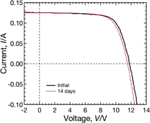
Fig. 4. I–V curve of the module, with the same composition as Sample A, heated at 85 °C during 14 days without PID stress.
Download figure:
Standard image High-resolution imageFigure 5 shows the dark I–V characteristics of Sample A before and after the PID tests. The shunt resistance Rsh is almost unchanged until the PID-stress duration reaches 7 days and slightly decreases after the PID test for 14 days. In a previous study,1) PID of p-type c-Si modules is characterized by a reduction in Rsh. The behavior of Rsh in the CIGS module is unlike that in c-Si modules. A slight increase in the series resistance Rs can also be observed from 3 to 7 days of PID-stress duration. These indicate that the CIGS modules degrade by different mechanisms in the case of c-Si modules.
Download figure:
Standard image High-resolution image
Fig. 5. (a) Dependence of the dark I–V characteristics of Sample A on PID-stress duration and (b) its semilog plot under forward bias. The PID tests were performed by applying −1000 V to connected submodule interconnector ribbons at 85 °C.
Download figure:
Standard image High-resolution imageOn the other hand, a significant increase in current can be observed under forward bias, as shown in Fig. 5(a). As can be seen in Fig. 5(b), Sample A simultaneously shows a significant increase in the ideality factor n under a forward bias of lower than 13 V. The n of each cell increases to approximately 9 from approximately 1.4 as a result of the PID test for 14 days.
n indicates the degree of recombination currents. However, on the basis of the well-known Shockley–Read–Hall (SRH) recombination model,26,27) n can reach but not exceed 2.28) This implies that the increase in n cannot be explained by the SRH recombination model assuming recombination via isolated defects. Here, we consider Steingrube's model29) in order to explain an n larger than 2 observed for the degraded CIGS PV module. Steingrube et al.29) have theoretically and experimentally demonstrated that recombination via coupled defect levels leads to n values larger than 2. From the model, the significantly higher n observed in our experiment can be due to an enhanced recombination induced by a very high defect density introduced into the depletion region in CIGS PV cells. Such a high defect density may be possible when impurities introduced into CIGS during PID tests are segregated at crystal defects or faults (which will be discussed in Sect. 3.2). n values larger than 2 have been observed for PID-affected c-Si modules11) and have been found to be attributed to defect levels introduced by Na impurities localized in stacking faults.10)
From the above discussion, it is implied that the degradation behavior of CIGS modules can be mainly characterized by an enhanced recombination. However, a slight increase in Rs and a slight decrease in Rsh might also to some degree affect the degradation.
A kink observed near 14 V for the unaffected sample may be a roll-over effect30) of cells included in the submodule, and then becomes inconspicuous after 3 days of the PID test. Such a roll-over behavior appears to be due to the second junction at the CIGS/Mo back interface.30) Kohara et al.31) have reported that MoSe2 enabling the ohmic contact at the CIGS/Mo interface only forms if Na is present. The disappearance of the roll-over behavior might be attributed to additional introduction of Na into the CIGS/Mo interface from the glass substrate side promoted by a relatively high temperature of 85 °C and a weak electric field during the PID test.
Figure 6 shows the dependence of η/η0 of Samples A, B, and C on PID-stress duration. As can be seen, the η/η0 of Sample A decreases to 0.2 after PID tests for 14 days in total, whereas that of Sample B is almost unchanged. This observation implies that the degradation of Sample A can be attributed to alkali metal ions, e.g., Na+, existing in the cover glass as in the case of c-Si PV modules. It also indicates that the influence of Na contained in the glass substrate and light-absorbing layer on the degradation can be neglected in our PID test. In addition, η/η0 of Sample C is almost unchanged, which suggests that the IO encapsulant can prevent PID of CIGS. The IO encapsulant is effective for preventing PID for at least 28 days under this experimental condition, since Sample C maintained a η/η0 of 1 after the PID test for 28 days. We have not conducted PID tests of Sample C exceeding 28 days. This shows that the use of high-electrical-resistance thermoplastic IO encapsulant is useful for preventing PID of CIGS modules as in the case of PID of c-Si modules.4,12)
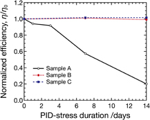
Fig. 6. Relationship between PID-stress duration and the normalized energy conversion efficiency η/η0 for Samples A–C. Sample A has standard components. On the other hand, Sample B has the non-alkali cover glass instead of the conventional tempered glass, and Sample C has the IO encapsulant instead of the EVA encapsulant.
Download figure:
Standard image High-resolution imageFigure 7 shows the EL images of unaffected and degraded CIGS modules (Sample A). Uniform luminescence can be observed in the EL image of the unaffected sample [Fig. 7(a)]. On the other hand, the EL image after the PID test for 7 days looks darker over the entire surface, and is significantly darkened in the upper and lower edges of the submodule [Fig. 7(b)]. In addition, the left side of the individual cells shows asymmetrically larger darkened areas. The EL completely disappeared after the PID test for 14 days [Fig. 7(c)]. These indicate that degradation uniformly proceeds over the entire surface except for the edges of submodules in our test setup. As asymmetry of darkened areas can be observed on the individual cells, the spread of degradation may be affected by scribing lines. As illustrated in Fig. 1(b), the structure on the left side of the scribing lines differs from that on the right side of the scribing lines, and, on the left side, CIGS and CdS layers are not covered by the ZnO layers. A low intensity of EL in general is attributed to shunts,32) high series resistance,33) and small diffusion length.34) It is, however, difficult to separate their influences from our EL results.
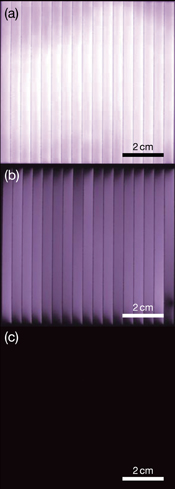
Fig. 7. EL images of Sample A (a) before PID test and after PID test for (b) 7 and (c) 14 days. The images were recorded at a bias current density of about 25 mA/cm2.
Download figure:
Standard image High-resolution imageIt has not been understood, at present state, how long the PID stress corresponds to the duration that generates PID in outdoor large-scale PV systems, and there are few attempts35) of clarifying the relationship between the PID acceleration test and actual PID observed outdoors. In the future, we will have to clarify them, by comparing the results of acceleration tests with those of field tests.
3.2. Diffusion behavior of Na
Figure 8 shows the D-SIMS depth profiles of Zn, Cd, Ga, and Na in CIGS modules with the same components as Sample A. The Zn, Cd, and Ga profiles indicate the locations of the interfaces of the ZnO, CdS, and CIGS layers. The Na profiles are shown for both unaffected and degraded samples. As can be seen from Fig. 8, the Na signal intensity in the ZnO layer of the degraded sample is higher than that of the unaffected sample. Moreover, the intensity seems to increase in the superficial region of the CdS layer of the degraded sample. In contrast, the Na signal intensity in the other layers is almost unchanged before and after the PID tests. Probably, these Na atoms or ions migrate from the module cover glass during PID stress. This observation implies that Na atoms or ions can migrate toward the cell and accumulate in the ZnO layer and the superficial region of the CdS owing to high voltage.
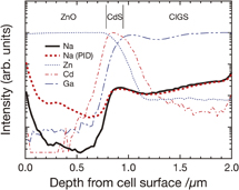
Fig. 8. (Color) D-SIMS depth profiles of Zn, Cd, Ga, and Na in the CIGS module with the same components as Sample A. The profiles are obtained using the Cs+ primary ion beam. The Zn, Cd, and Ga profiles indicate the locations of the interfaces of ZnO, CdS, and CIGS layers. The Na profiles are shown for both unaffected and degraded (η/η0 = 0.3) samples. Note that the ordinate is on a log scale.
Download figure:
Standard image High-resolution imageThe Na concentration slightly increases in the superficial layer of the CdS layer. A significant increase in Na signal intensity cannot be, however, observed in the CdS and CIGS layers. It cannot be denied that a few Na atoms introduced into the CdS or CIGS layer from the cover glass lead to an enhanced depletion region recombination. Actually, it is stated that, for c-Si modules, even small volume fractions of Na can lead to high areal concentrations when it is piled up in planes, such as stacking faults.10) Even for PID of CIGS modules, the degradation might be affected by defects and/or faults, which can lead to a local high density of Na. Grain boundaries in the CIGS layer might be one of the candidates for such defects or faults. Cojocaru-Mirédin et al.36) have reported that Na impurities are segregated at the grain boundaries in CIGS. In addition, too much doses of Na have been found to have detrimental effects on Voc and FF.37–39) However, at the present state of our research, we have not yet obtained results that explain the effects of defects and/or faults including grain boundaries.
Substitutional Na (NaZn) can produce deep acceptor levels in ZnO semiconductors,40) and can increase the electrical resistivity of n-ZnO semiconductors by carrier compensation.41) Figure 9 shows the scanning capacitance microscopy images of CIGS modules with the same composition as Sample A before and after the PID test for 21 days. Stripes in the Mo layer are not essential but originate from multiple depositions of the Mo layer. A decrease in the signal intensity of the ZnO layer means a decrease in carrier concentration, which suggests the carrier compensation by Na diffusion. However, neither the destruction nor disappearance of the p–n junction is observed even after the PID test. A slight increase in Rs observed in Fig. 5(a) may also be attributed to the doping of the ZnO layer with Na. However, ZnO includes intrinsic donor defects, the so-called "hole killers" leading to strong self-compensation, e.g., interstitial Zn (Zni) and oxygen vacancies (VO).42) In addition, group-I impurities at interstitial sites can be electron donors.43) These suggest that NaZn may also be compensated for in the ZnO layer by the intrinsic defects and/or coexisting interstitial Na (Nai). If this is the case, the decrease in Rs might be mainly caused by the decrease in mobility due to impurity scattering.44)

Fig. 9. (Color) Scanning capacitance microscopy images of CIGS modules with the same composition as Sample A (a) before and (b) after the PID test for 21 days. Dark areas indicated by dashed circles originate from mechanical polishing or organic contamination during sample preparation.
Download figure:
Standard image High-resolution image3.3. Influence of positive bias applied to degraded CIGS modules
Table II shows the performance, such as the normalized open circuit voltage Voc/Voc,0, the normalized short circuit current Isc/Isc,0, the normalized fill factor FF/FF0, and η/η0, of a sample degraded by the PID test for 7 days and the performance recovered by application of a positive bias of +1000 V for 7 days. The sample has the same composition as Sample A. As listed in Table II, all normalized parameters reach 0.95 and higher after applying a positive bias of +1000 V. In other words, the degraded module almost completely recovers from its performance loss by applying a positive bias. This result reveals that, as in the case of c-Si modules,1,18,19) the PID-affected CIGS modules can recover from the degradation by applying a positive bias.
Table II. Normalized performance of the sample subjected to PID test for 7 days and the one recovered by a positive bias of +1000 V for 7 days.
| Condition | Voc/Voc,0 | Isc/Isc,0 | FF/FF0 | η/η0 |
|---|---|---|---|---|
| Degraded | 0.59 | 0.98 | 0.44 | 0.25 |
| Recovered | 0.98 | 1.00 | 0.97 | 0.95 |
Table III shows Voc/Voc,0, Isc/Isc,0, FF/FF0, and η/η0 of Sample A after the PID test for 14 days and nine months after the PID test. Sample A has been left at room temperature after the PID test. All parameters return to baseline values nine months after the PID test, indicating that degraded CIGS modules can gradually recover from their performance losses at room temperature without voltage bias. This also implies that CIGS modules may also gradually recover in very large-scale systems, e.g., at night. This recovery phenomenon has been reported on a cell level by Fjällström and coworkers.23,45)
Table III. Normalized performance of Sample A after the PID test for 14 days and nine months after the PID test. During nine months, Sample A has been left at room temperature without voltage bias.
| Condition | Voc/Voc,0 | Isc/Isc,0 | FF/FF0 | η/η0 |
|---|---|---|---|---|
| Degraded | 0.50 | 0.95 | 0.42 | 0.20 |
| Recovered | 0.98 | 1.00 | 0.98 | 0.97 |
The above results reveal the reversibility of PID of CIGS modules. The recovery in CIGS modules may be explained by the out-diffusion of alkali metals, such as sodium, as in the case of c-Si PV modules, since PID can be attributed to accumulation of alkali metals. When a positive bias is applied to interconnector ribbons of CIGS modules, Na, which is present in the encapsulant, may go back toward the cover glass with assistance from the applied bias and thermal energy. This may lead to a Na concentration gradient between the submodule and the encapsulant, enabling out-diffusion of Na accumulated in cells. For the recovery phenomenon at room temperature, the Na impurities with high-density accumulating in the encapsulant and the CIGS cells might go back toward the cover glass side with assistance from the thermal energy at room temperature. However, it is not clear, at the present state, why the recovery phenomenon strongly occurs even at room temperature without voltage bias.
3.4. PID resistance of CIGS modules
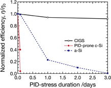
Figure 10 shows the dependence of η/η0 of the CIGS module (Sample A), PID-prone multicrystalline Si modules, and a thin-film a-Si module on the PID-stress duration. The values of η/η0 of the PID-prone multicrystalline Si module decrease to 0.05–0.4 after the PID test for 2 h, and the a-Si module shows total failure after the PID test for 3 days. In contrast, the η/η0 of the CIGS PV module is maintained near 1 after PID test for 3 days. This reveals that the CIGS modules have a higher PID resistance than the PID-prone multicrystalline Si and a-Si modules. A possible reason for the higher PID resistance may be that the permissible number of impurities in CIGS PV cells is higher than that in Si PV cells. In addition, low doses of Na impurities rather significantly increase Voc and FF of CIGS PV cells.46,47) In contrast, Na is one of the very deleterious elements in Si, which introduces a level close to the mid-gap and has large capture cross sections.48)
Fig. 10. Relationship between duration of PID stress and normalized energy conversion efficiency η/η0 of the CIGS module (Sample A), multicrystalline Si modules, and a thin-film a-Si module.
Download figure:
Standard image High-resolution image
Note that our PID tests are severe as can be seen from the results of the multicrystalline Si modules. PID of CIGS modules might not be a serious problem, since after the PID test for 3 days, the c-Si and a-Si modules show the total failure while the CIGS module maintains a η/η0 of about 0.9. PID can be prevented by using high-resistance thermoplastic encapsulants, e.g., IO, as shown in Fig. 6, even if CIGS modules are deployed in significantly severe fields. We have not, however, investigated the influence of high humidity on PID behavior. For thin-film Si PV modules, corrosion of their SnO2 transparent conducting oxide layers at a high humidity has been reported.20) Investigations on the influence of humidity on PID of CIGS modules should be conducted to further obtain the knowledge of the reliability of CIGS modules.
4. Conclusions
Using the PID acceleration test on module level, we investigated PID of CIGS modules fabricated from integrated submodules. The CIGS modules have suffered from PID. From our results, we have reached following conclusions:
- (1)CIGS modules suffer PID under this experimental condition.
- (2)PID of CIGS modules can be attributed to alkali metals, e.g., Na, migrating from the cover glass.
- (3)Na migrating from the cover glass mainly accumulates in the n-type ZnO transparent conducting layer. However, Na impurities might be segregated at the crystal defects and/or faults in multicrystalline thin films such as the CIGS layer.
- (4)PID of CIGS modules may be mainly influenced by the enhancement of recombination in their p–n junctions.
- (5)IO encapsulants can prevent PID of CIGS modules. The IO encapsulant is effective for preventing PID for at least 28 days under this experimental condition.
- (6)Degraded CIGS modules can recover from the degradation after applying a positive bias.
- (7)CIGS thin-film PV modules have high resistance to PID compared with multicrystalline and a-Si modules.
Acknowledgments
The authors are grateful to Akimasa Yamada, Hideki Takahashi, Miwako Takano, Masayuki Iioka, and Hirofumi Higuchi of AIST for their help in submodule fabrication. The authors would like to thank Professor Keisuke Ohdaira of JAIST for helpful advice.