
Abstract
Thermoelectric devices convert heat energy to electric power. The dimensionless thermoelectric figure of merit, ZT, is used as a standard criterion for efficiency of thermoelectric conversion. This criterion requires a high Seebeck coefficient, a high electric conductivity, and a low thermal conductivity. In this regard, PbTe, BiTe, and their alloys consisting of relatively heavier elements have been found to show higher values of ZT. In this paper, we focus on the potential of graphene-based composites as thermoelectric materials. Graphene was considered to be a disadvantageous material because of its extremely high thermal conductance and relatively low Seebeck coefficient. However, it has been reported recently that a structural modulation is an effective way of raising the thermoelectric ability of graphene. We introduce the recent progress in the design of graphene-based materials for thermoelectric devices. In particular, we provide a focused investigation of our recent progress regarding the thermopower enhancement in nanoarchitectonics, superlattices, and composites consisting of graphene and hexagonal BN nanoribbons. It has been shown that low-dimensional modulations are effective ways of obtaining a high thermoelectric performance of graphene-based materials.
Export citation and abstract BibTeX RIS
1. Introduction
Thermoelectric effects are applicable to the conversion of heat energy to electric power. The dimensionless thermoelectric figure of merit, ZT, is commonly used as an index of efficiency of thermoelectric conversion, which is defined by
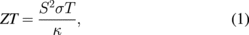
where S is the Seebeck coefficient, σ is the electric conductivity, κ is the thermal conductivity due to both electrons and phonons, and T is the absolute temperature. Here, ZT ≥ 1 is a standard criterion for practical use. However, it has been difficult to obtain a sufficiently high figure of merit to meet such a criterion, because it is simultaneously needed to reduce κ and to raise σ and S. In previous decades, PbTe, BiTe, and their alloys consisting of relatively heavier elements were found to show relatively higher values of ZT (∼1).1) Some of such first-generation materials consist of rare metals or have high toxicity; thus, more eco-friendly and clean thermoelectric materials had been desired. However, the development of new alternative materials that surpass those alloys did not progress for several decades. Hicks and Dresselhaus, however, showed that quantum-well structures, that is, two-dimensional (2D) layer structures, can significantly modify and greatly improve the thermoelectric figure of merit.2) Furthermore, they insisted that one-dimensional (1D) conductors such as quantum wires potentially show significant increases in ZT compared with both the bulk and 2D structures.3) Such predictions motivated the development of new kinds of thermoelectric materials with low-dimensional configurations, including Bi2Te3/Sb2Te3,4) SiGe/Si,5) and In0.53Ga0.47As/In0.53Ga0.28Al0.19As superlattices.6)
Graphene, a single-atomic-layer graphite, which has a 2D form of carbon, has been found to exhibit high crystal quality and anomalous properties such as high electron mobility.7) Therefore, graphene-based materials have attracted much attention as a candidate for next-generation electronic materials. In contrast, graphene is quite disadvantageous as a thermoelectric material because of its extremely high thermal conductance8–11) and relatively low Seebeck coefficient (∼80 µV/K at room temperature).12,13) Recently, however, it has been suggested that graphene-based devices with a periodic nanostructure show a Seebeck coefficient higher than 30 mV/K.14) This means that modulated graphene has a high potential to be used as a promising thermoelectric material.
Graphene nanoribbons (GNRs) have also been extensively studied,15–17) since their electronic structure can be controlled by modifying both the edge shape and ribbon width, similarly to carbon nanotubes. It has been demonstrated that zigzag GNRs (ZGNRs) show magnetic ground states resulting from the so-called zigzag edge states,15,18–20) or the electric-field-induced half-metallicity.21) Recently, GNRs and their modulated structures have also been investigated as thermoelectric materials. For example, Ouyang and Guo reported that the maximum magnitude of the Seebeck coefficient of an armchair edge GNR is much higher than that of graphene, which is on the order of mV/K.12) Such a demonstration implies that the introduction of a linear modulation to graphene makes it possible to increase its thermoelectric ability, as predicted by Hicks and Dresselhaus.2,3) In this paper, we provide an overview of the development of thermoelectric materials consisting of graphene and its low-dimensional derivatives. In particular, we discuss the mechanism of the enhancement of Seebeck coefficient in heterographene superlattices22) and graphene nanocomposites.
2. Seebeck coefficients of graphene and graphene nanoribbons
In this section, we take up graphene and GNRs and present an overview of their potential as thermoelectric materials. Graphene was not considered to be applicable to thermoelectric conversion. Although the high carrier mobility of graphene is an advantage in the context of the thermoelectric figure of merit, the main drawbacks are its extremely high thermal conductance and relatively low Seebeck coefficient. The thermal conductance of graphene was measured at room temperature, and it was close to the ballistic thermal conductance, up to 5000 W/(m·K),8–11) which surpasses that of diamond. It has been reported that experimental values of the Seebeck coefficient of graphene are 30–80 µV/K.8,13,23) From the theoretical point of view, the peak value of the Seebeck coefficient simulated at the ballistic limit is close to the experimental value,12) corroborating the large electron mean-free path in graphene.7) Figure 1 shows the simultaneously measured conductivity and thermoelectric power (TEP), namely, Seebeck coefficient, of graphene at various temperatures as a function of gate voltage.13) The profile of TEP showed asymmetric behavior with regard to the sign of gate voltage, indicating that the majority carriers change from holes to electrons across the zero gate voltage. As shown in the inset of Fig. 1, the magnitude of TEP increased linearly with increasing temperature. The authors gave an explanation for such a linear temperature dependence of TEP: The thermopower in graphene is dominated by diffusive conduction24) rather than the phonon drag.25) At approximately the same time, Checkelsky and Ong26) and Wei et al.23) also demonstrated the thermopower of a single layer of graphene. All measurements showed that the peak TEP is about 80 µV/K. As a result, the ZT of graphene would be estimated to be only 0.006 at room temperature.27)

Fig. 1. (a) Conductivity and (b) TEP of a graphene sample as a function of Vg at T = 300 K (square), 150 K (circle), 80 K (up triangle), 40 K (down triangle), and 10 K (diamond). Upper inset: Scanning electron microscopy image of a typical device; the scale bar is 2 µm. Lower inset: TEPs taken at Vg = 30 V (square) and −5 V (circle). Dashed lines are linear fits to the data. Reprinted with permission from Ref. 13. © 2009 American Physical Society.
Download figure:
Standard image High-resolution imageRecently, however, it has been theoretically estimated that a graphene-based device with a kind of periodic nanostructure shows a Seebeck coefficient higher than 30 mV/K.14) Figure 2 shows the thermoelectric graphene device14) with an enhanced Seebeck coefficient. In this device, metallic electrodes were periodically patterned over graphene deposited on a silicon dioxide substrate. It was concluded that the modulated graphene has a huge potential to be a promising thermoelectric material. Along this line, 1D graphene, GNRs, and their derivatives have also been tested as thermoelectric materials. Ouyang and Guo investigated the thermopower of graphene and 1D armchair GNRs (AGNRs) using the nonequilibrium Green's function method.12) They reported that the maximum Seebeck coefficient of AGNRs is much higher than that of graphene, which is on the order of mV/K, as shown in Fig. 3(a). Kato et al. also suggested that AGNRs exhibit a much higher Seebeck coefficient on the order of mV/K than ZGNRs, and the Seebeck coefficients of AGNRs are classified into three categories depending on the width of the ribbons.28) Indeed, an extremely high ZT = 6 was demonstrated by a molecular dynamics study, which is due to a high Seebeck coefficient for AGNRs such as S ∼ 4 mV/K.29) The higher ZTs of AGNRs than those of ZGNRs are also attributed to a lower lattice thermal conductance of AGNRs.30,31)

Fig. 2. Thermoelectric graphene device with an enhanced Seebeck coefficient. Reprinted with permission from Ref. 14. © 2007 AIP Publishing.
Download figure:
Standard image High-resolution image
Download figure:
Standard image High-resolution image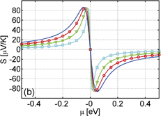
Fig. 3. Comparison of 1D GNR with 2D graphene: the thermopower of (a) a perfect n = 15 AGNR and (b) a 2D graphene as a function of μ (chemical potential) at different temperatures: T = 75 K (squares), 150 K (triangles), 225 K (circles), and 300 K (unmarked). In (a), the dashed line indicates the first conduction subband edge EC. The inset shows the enlarged parts for μ > EC. Reprinted with permission from Ref. 12. © 2009 AIP Publishing.
Download figure:
Standard image High-resolution imageOn the other hand, to reduce thermal conduction, several works suggested the introduction of lattice vacancy defects,29,32) isotopes,33–35) antidots (nanomeshes),36) junction structures,37,38) external stress,39) external electric field,40) and kinks.30,41) A GNR–annulene–GNR junction was predicted to have a ZT of ∼0.5 and a Seebeck coefficient of ∼150 µV/K at room temperature,37) which result from the suppression of phonon transport at the junction. It was reported that AGNRs with the chevronlike structure have ZTs of up to 0.6.30) Furthermore, the ZT of ZGNRs, which is nearly equal to zero, was significantly improved by the introduction of the chevronlike structure.30) Figure 4 shows the structural models proposed by Huang et al., the chevronlike structure with two types of segments, that is, AGNR and ZGNR.30) The thermoelectric performance of such kinked GNRs can be enhanced compared with that of straight GNRs. It is interesting to note that the kinked GNRs with zigzag edges show a thermoelectric ability comparable to those with armchair edges, whereas the ZT of the straight ZGNR is nearly equal to zero. Huang et al. also suggested that thermoelectric performance degrades with increasing length of the zigzag segment, because the bandgap of the kinked GNRs decreases accordingly. This suggests that the bandgap opening with modulated structures of ZGNRs may significantly enhance the thermoelectric ability of ZGNRs. It was also predicted that ZGNR with linearly aligned defects has an extremely high ZT of up to ∼5 at maximum.29) Regardless of whether a higher Seebeck coefficient or a lower lattice thermal conductance should be more essential for obtaining a higher ZT of AGNRs or not, such demonstrations imply that the introduction of a linear modulation to graphene makes it possible to increase the thermoelectric performance.

Fig. 4. Structures of kinked  AA/ZZ-GNRs with two segments with the same edge shape, i.e., armchair or zigzag, connected by 120°, and kinked AZAZ/ZAZA-GNRs with two segments with different edge shapes connected by 150° with a horizontal armchair-zigzag segment. For AA- and ZZ-kinked GNRs, the length of the arm is defined by the index l, the width of the kink by the index w, and the width of the arm by d. Transport is along the horizontal direction. Reprinted with permission from Ref. 30. © 2009 American Physical Society.
Download figure:
Standard image High-resolution imageRecent progress in the development of experimental techniques enables us to fabricate hybrid 2D monolayers consisting of graphene and hexagonal BN (h-BN).42–48) Figure 5 shows a successful demonstration of the fabrication using a bottom-up approach:46) Graphene and h-BN were sequentially grown on Ru(0001) by lateral heteroepitaxy. Very recently, the electronic properties at the graphene/h-BN interface have been observed experimentally49–51) and revisited theoretically.19,52–55) It was also estimated theoretically that the phonon thermal conductivity is significantly reduced in the graphene/h-BN superlattice56,57) and hybrid structures57,58) compared with pristine graphene. It was pointed out that lateral strain affects the transmission of phonons at the graphene/h-BN interface.59) Yang et al. estimated theoretically the thermoelectric properties of the graphene/h-BN hybrid structure and demonstrated the enhancement of ZT because of the reduced phonon transmission.60) Furthermore, Yokomizo and Nakamura showed that the hybrid superlattice consisting of ZGNRs and zigzag BN nanoribbons (ZBNNRs) has a giant Seebeck coefficient on the order of mV/K,22) even though the pristine ZGNRs are not suitable as a thermoelectric material.30) Such an enhancement of the Seebeck coefficient is attributed to the formation of the finite band gap and the presence of the so-called flat band at the band edge.15,16,61) The mechanism of this anomalous enhancement in the superlattice having a zigzag interface is described in detail in the following section.

Fig. 5. Lateral heteroepitaxy of 2D materials on a metal support. (a) Schematic representation of the sequential growth of boron nitride and graphene by lateral heteroepitaxy at the edge of a 2D seed crystal (here, a metal-supported graphene flake). (b–g) Real-time microscopy of the stepwise growth of a monolayer superlattice of alternating graphene (G) and boron nitride (BN) stripes by exposure of a Ru(0001) substrate to ethylene (C2H4) and borazine (B3H6N3), respectively. Substrate temperature: 750 °C. (h) Time-dependent pressure of precursor gases. (i) Measured width of the graphene and boron nitride stripes normalized to the integrated precursor gas dose used for the growth of each stripe. Reprinted with permission from Ref. 46. © 2014 American Chemical Society.
Download figure:
Standard image High-resolution image3. Seebeck coefficient of the GNR/BNNR superlattices
In this section, we shall focus on the effects of the introduction of quasi-1D modulations on the thermal property and show that ZGNR/h-BN superlattices markedly enhance the Seebeck coefficients of ZGNRs.22) Here, the superlattice models consisting of ZGNRs and ZBNNRs are proposed. We follow the conventional nomenclature to describe the system uniquely. In this manner, we use a pair of integers  , which are the numbers of dimer lines of ZGNR and ZBNNR in the unit cell of the superlattice, respectively. Figure 6 shows the structure of the
  superlattice as an example. In this study, we focus on smaller systems with n + m ≤ 8 for simplicity; it has been shown that carbon atoms doped in a BN sheet can form 1D nanoribbons under suitable chemical conditions,55) and small systems with n + m ≤ 8 have nonmagnetic ground states and direct gaps.62) We employed the ab initio calculation based on the density functional theory63) to evaluate the electronic structures of the superlattices. The results were obtained using the program code abinit.64,65) Detailed calculation conditions can be found in the literature.22) For all the combinations of
  such that n + m ≤ 8, ZGNR/BNNRs were confirmed to be direct-transition semiconductors with finite bandgaps.

Fig. 6. Structure of  ZGNR/BNNR; the black, white, and gray balls indicate C, B, and N atoms, respectively. Reprinted with permission from Ref. 22. © 2013 AIP Publishing.
Download figure:
Standard image High-resolution imageFigure 7 shows the band structure of the  superlattice as a representative example. The dispersion relation for the
  superlattice is similar to that for the ZGNR near the Fermi energy, except for the bandgap: 0.25 eV for ZGNR (n = 2) and 0.80 eV for the
  superlattice. Such characteristics hold for the other systems with different
  combinations. It has been reported that the bandgap opens in ZGNR under the static electric field.21) Hence, the bandgap widening of the ZGNR/BNNR is attributed to an inner electric field induced at the GNR/BNNR polar interface. Figures 8(a) and 8(b) show the Seebeck coefficients calculated for the ZGNR/BNNR superlattices and the isolated ZGNRs at room temperature, respectively. The Seebeck coefficients calculated for the AGNR/BNNR superlattices and the isolated AGNRs at room temperature are also shown in Figs. 8(c) and 8(d) for comparison. As clearly seen, ZGNR/BNNRs have higher Seebeck coefficients than ZGNRs. In particular, the
  superlattice has the maximum Seebeck coefficient of 1.78 mV/K, while ZGNR (n = 2) has the Seebeck coefficient of 0.282 mV/K; the Seebeck coefficient of the superlattice is 6.3 times higher than that of ZGNR, and 22 times as high as that of graphene.12,13) Such giant Seebeck coefficients of the superlattices are derived from their distinct band structures. As shown in Fig. 7, the superlattice exhibits the pudding mold band66) near the band edge, in which the mobility of carriers is much higher than that of counter carriers. This is the reason for the enhancement of the Seebeck coefficients of the ZGNR/BNNR superlattices. From this point of view, pristine ZGNR is also expected to show a high Seebeck coefficient, because ZGNR shows the so-called flat band near the Fermi level15,16) similar to the pudding mold band. However, its actual Seebeck coefficient has been reported to be not so high.29,30,67) The ZGNR exhibits a semimetallic band structure;61) thus, the one-band model2) no longer holds. Therefore, if the bandgap is opened without the modification of the shape of the band edge, the Seebeck coefficient of ZGNR is enhanced. Such a perspective can be one of the guiding principles for designing other materials with high Seebeck coefficients. On the other hand, AGNRs do not have a pudding mold band. Hence, such a mechanism to raise the Seebeck coefficient does not work for AGNRs. In fact, the Seebeck coefficient of
  AGNR/BNNR becomes lower, not higher than that of the free-standing AGNR (n = 2), as shown in Figs. 8(c) and 8(d).

Fig. 7. Band structure of  ZGNR/BNNR; the energy origin was set to the top of valence band; Γ → X direction corresponds to the ribbon axis direction, Γ → Y corresponds to the direction perpendicular to the ribbon axis. Reprinted with permission from Ref. 22. © 2013 AIP Publishing.
Download figure:
Standard image High-resolution image
Fig. 8. Seebeck coefficients of (a) the ZGNR/BNNR superlattices, (b) free-standing ZGNRs, (c) AGNR/BNNR superlattices, and (d) free-standing AGNRs at 300 K as a function of the chemical potential experienced by electrons. Reprinted with permission from Ref. 22. © 2013 AIP Publishing.
Download figure:
Standard image High-resolution imageNow that the enhancement of the Seebeck coefficient has been confirmed for the superlattices, the role of BNNRs in the superlattice structure should be clarified. The Seebeck coefficients of ZGNRs are not very high, because the carrier flux generated by heat energy is compensated by the counter carrier flux, which stems from the two nearly degenerate flat bands of ZGNRs at E − μ = 0. Here, the question arises about what dominates the Seebeck coefficient of these systems. The BNNRs in the ZGNR/BNNRs have polarity and generate the inner electric field at the interface between ZGNRs, which results in the expansion or opening of the bandgaps of ZGNRs. This is actually the so-called electric field effect reported by Pruneda.62) Figure 9 shows the relationship between the maximal, absolute Seebeck coefficient and bandgap at various temperatures. As clearly seen in this figure, the Seebeck coefficient shows an obvious linear dependence. Such a positive correlation is associated with the fact that the one-band model holds better in the systems with wider bandgaps; the less compensation by counter carriers in the wide-bandgap systems results in the increase in the Seebeck coefficient. Hence, the modulated structures of ZGNRs, which have larger bandgaps, could provide a higher Seebeck coefficient, if the characteristic of the pudding mold band remains unchanged.

Fig. 9. Relationship between maximal, absolute Seebeck coefficient and bandgap for the ZGNR/BNNR superlattices. Squares, circles, and triangles show the Seebeck coefficients at 150, 300, and 450 K, respectively. Reprinted with permission from Ref. 22. © 2013 AIP Publishing.
Download figure:
Standard image High-resolution imageIn this section, we introduce our recent study.22) The Seebeck coefficients of the ZGNR/BNNR superlattices are higher than those of ZGNRs within the framework of ab initio calculations based on the density functional theory. In particular, the Seebeck coefficient of  ZGNR/BNNR is 6.3 times higher than that of ZGNR (n = 2). This means that the figure of merit (ZT) can become 39 times higher, if the transport properties of ZGNR/BNNR, such as electric and thermal conductivities, remain unchanged from those of ZGNR. It has been reported that the ZTs of n-ZGNRs become 1.1–1.7 for n = 3–6;67) thus, it is expected that the ZT of ZGNR/BNNR exceeds 39. Such an expectation seems to be too optimistic. However, the electrical conductivities of the superlattices can remain unchanged from those of pristine ZGNRs, because the number of π-bands contributing to the Seebeck effect is unity under certain chemical potentials at which the one-band model holds. On the other hand, the lattice thermal conductivities of pristine GNRs are higher than that of graphene, regardless of their edge structures such as zigzag or armchair.31) These extremely high thermal conductivities of GNRs are due to the existence of the fourth acoustic mode in the phonon dispersions of GNRs, which originates from the one dimensionality of GNRs. Therefore, the thermal conductivities of ZGNR/BNNR superlattices can be reduced to values comparable to that of graphene because of the two dimensionality of the superlattices. Our estimation of ZT is, in light of these prospects, more pessimistic rather than optimistic. Hence, ZGNR-based modulated structures having the pudding mold band with wider bandgaps have the potential as the fully light-element-based thermoelectric materials with extremely high figures of merit.
4. Seebeck coefficients of the BN-terminated GNR
It would be quite difficult to fabricate the 2D superlattice described in the preceding section. Thus, in this section, we explore the electronic structure and the Seebeck coefficients of GNRs with edges terminated by BNNRs, which could be manufactured more easily. The graphene boron nitride nanoribbons (GBNNRs) are composed of GNRs sandwiched between BNNRs. The edges of BNNRs are terminated with hydrogen atoms. We considered GBNNRs with zigzag edges (ZGBNNRs) and GBNNRs with armchair edges (AGBNNRs). As in the previous section, we use a pair of integers  , which are the numbers of dimer chains of GNRs and BNNRs, respectively. As an example, the GBNNRs of
  are shown in Fig. 10. For the lattice constant in the direction along ribbons (x-direction in Fig. 10), we adopted those of graphene, namely, 2.462 Å for ZGBNNRs and 4.264 Å for AGBNNRs. The results in this section were obtained using the vasp code.68,69) The wave function was expanded with a plane-wave basis set with an energy cutoff of 400 eV. Periodically arranged ribbons under the boundary condition were separated by 12 Å, which was sufficiently large to prevent interactions between adjacent ribbons. The generalized gradient functional given by Perdew et al. was utilized as the exchange–correlation functional.70) The ultrasoft pseudopotentials were generated using the Vanderbilt strategy.71) Integration over the 1D Brillouin zone (BZ) was performed by 30-k-point sampling in the irreducible BZ. Structural optimization with respect to ionic positions was performed until each component of interatomic forces became less than 1.0 × 10⁻² eV/Å.

Fig. 10. Calculation models of (a) ZGBNNR  and (b) AGBNNR (4,4). The black, white, gray, and light gray balls indicate C, B, N, and H atoms, respectively.
Download figure:
Standard image High-resolution image4.1. ZGBNNR
Figure 11(a) shows the energy band structure of ZGBNNR  . Such a narrow ZGBNNR with a relatively small n has a finite energy gap. The highest occupied valence band and the lowest unoccupied conduction band become flat near the X point. This band shape is similar to the pudding mold band structure, as seen in the previous section. The internal electric field between GNRs and BNNRs widens the energy gap and, thus, hinders the compensation by the counter carriers. Table I shows the energy gaps of ZGBNNRs. As the GNR width n increases, the energy gap decreases since the effect of the internal electric fields becomes smaller. The change in band gap with respect to the BNNR width m exhibits a relatively small widening for m = 4 and saturates for m = 6. These results indicate that the strength of the electric field in GNR-BNNR boundaries hardly varies for m > 4.

Fig. 11. (a) Band structure of ZGBNNR  . The red dotted line indicates the middle between the valence band top and the conduction band bottom. (b) Seebeck coefficients of ZGBNNRs with m = 4 at 300 K as a function of chemical potential. (c) Relationship between the maximal Seebeck coefficient and the energy gap of ZGBNNRs with m = 4.
Download figure:
Standard image High-resolution imageTable I. Energy gaps of ZGBNNRs (eV).
| System | ΔE | System | ΔE | System | ΔE |
|---|---|---|---|---|---|
 |
0.547 |  |
0.617 |  |
0.617 |
 |
0.145 |  |
0.220 |  |
0.202 |
 |
0.026 |  |
0.085 |  |
0.082 |
 |
0.014 |  |
0.023 |  |
0.015 |
 |
0.013 |  |
0.004 |  |
0.001 |
Figure 11(b) shows the Seebeck coefficient as a function of the chemical potential for ZGBNNRs with m = 4 at 300 K. The existence of the pudding mold band with a finite energy gap enhances the Seebeck coefficient. The maximal Seebeck coefficient is 947 µV/K for ZGBNNRs  . As compared with the maximal Seebeck coefficient of hydrogen-terminated ZGNRs with n = 2 [see Fig. 8(b)], that is, 282 µV/K, it is confirmed that the Seebeck coefficient of ZGBNNR becomes more than three times higher than that of the pristine GNR. The increase in the maximal Seebeck coefficient with a relatively large BNNR width (m > 4) is small, since the band gap is small. This behavior is simply explained by the relationship between the maximal Seebeck coefficient and the energy gap shown in Fig. 11(c). The maximal Seebeck coefficient is proportional to the band gap, exhibiting a one-to-one correspondence, as shown in Fig. 11(c). As the temperature increases, the slope of the linear relationship becomes smaller.
4.2. AGBNNR
Figure 12(a) shows the Seebeck coefficient of AGBNNRs with m = 4 at 300 K as a function of the chemical potential. The maximal Seebeck coefficient is 2763 µV/K for AGBNNRs  , which is comparable to that of the pristine AGNRs [see Fig. 8(d)]. In the case of AGNRs, no effect of "boron nitride termination" on the Seebeck coefficient is found. Since the armchair edges of hexagonal boron nitrides are not polarized, the band gap remains unchanged under boron nitride termination. Hence, for both ZGNRs and AGNRs, the band gap opening is one of the key factors that contribute to the enhancement of the maximal Seebeck coefficient.

Fig. 12. (a) Seebeck coefficient of AGBNNRs with m = 4 at 300 K as a function of chemical potential. (b, c) Maximal Seebeck coefficient as a function of the width n of GNR for AGBNNRs with m = 4 and 6, respectively.
Download figure:
Standard image High-resolution imageIn order to examine how the maximal Seebeck coefficient varies as the ribbon width increases, we here classify AGBNNRs into three groups, 3n, 3n + 1, and 3n + 2, depending on the width (n) of GNRs. In Figs. 12(b) and 12(c), we show the Seebeck coefficient as a function of n for each group. It is clearly seen that the Seebeck coefficient decreases simply with increasing n for each group. This type of n dependence is also known for simple AGNRs,22,28) namely, monotonic decrease by grouping n by modulo 3.
As discussed above for ZGBNNRs, the Seebeck coefficient strongly depends on the band gap width and this relationship also holds for AGBNNRs. Figure 13 shows the maximal Seebeck coefficient as a function of the energy gap at several temperatures. As indicated by the black fitting line in each plot, one can clearly see the proportional relationship at each temperature within energy ranges that the Seebeck coefficients do not exceed a threshold value of about ∼2800 µV/K. Above this threshold, the Seebeck coefficient saturates even for the systems with a large band gap. Below the threshold, the maximal Seebeck coefficient is proportional to the band gap, as seen in the case of ZGBNNRs [see Fig. 11(c)]. This behavior is confirmed regardless of the width n of GNR. Here, we discuss the mechanism of the saturation of the Seebeck coefficient and the origin of the linear relationship. For systems with a narrow band gap, counter carriers of the highest occupied valence band (HOVB) and the lowest unoccupied conduction band (LUCB) compensate for each other, resulting in small contributions to the Seebeck coefficient from these two bands. Even for systems with a wider gap, if temperature is sufficiently high, the counter carrier compensation takes place as well. In Fig. 13(d), a schematic band structure near the Fermi level is shown, where the energy dispersions of HOVB and LUCB are almost symmetric. When the chemical potential is shifted from the middle of the gap, the contributions from HOVB and LUCB are unbalanced, giving rise to an increase in the Seebeck coefficient. If the bandgap increases beyond ∼2kBT, carrier compensation no longer takes place and only HOVB or LUCB contributes to the electron/hole transport. In this case, energy dispersions only near the valence band maximum or the conduction minimum dominate the carrier transport. Therefore, the Seebeck coefficient of AGBNNRs exhibits saturation behavior at lower temperatures and wider band gaps.

Fig. 13. (a), (b), and (c): Relationship between the maximal Seebeck coefficient and the energy gap of AGBNNRs with m = 4 for 100, 200, and 300 K, respectively. Linear fittings with the black lines are applied for the Seebeck coefficient data lower than 2500 µV/K. (d) Schematic of an effective band range that contributes to the Seebeck coefficient. The red dashed line indicates a chemical potential and the black dashed lines indicates energy ranges of (E − μ) ∼ ± kBT, below and above the chemical potential.
Download figure:
Standard image High-resolution image
5. Conclusions
We have reviewed the progress in research on the thermoelectric performance of graphene and graphene-based 1D/2D materials. Graphene has the characteristics of extremely high electric and thermal conductivities. In terms of the thermoelectric figure of merit, high thermal conductivity degrades significantly the thermoelectric performance of graphene. However, the foresight given by Hicks and Dresselhaus2,3) and the recent diversification of graphene-derived low-dimensional materials have stimulated our motivation to explore the new frontier of graphene families. Here, we have overviewed the potential use of pristine graphene, 1D GNRs and their derivatives, and 2D materials consisting of GNRs and BNNRs. Low-dimensional modulations are effective ways of obtaining the high thermoelectric performance of graphene-based materials. New types of low-dimensional materials have been discovered, which show fascinating thermoelectric properties, such as phosphorene72–74) and silicene and germanene.75) Transition metal dichalcogenides such as MoS2 and WSe2 are also revisited as thermoelectric materials in the monolayer form.74) Recently, on the other hand, the need for a new paradigm to describe thermoelectric properties has been confirmed under particular circumstances.76,77) Stimulated by the material design based on graphene, various types of low-dimensional materials will take prominence in the future.
Acknowledgments
The authors would like to thank Y. Yokomizo and Y. Ayako for helpful discussions.
Biographies

Jun Nakamura received his Ph.D. degree in Engineering from Waseda University in 1996. He worked as a research associate at Waseda University from 1995 to 1997, as a Postdoctoral Research Fellow of the Japan Society for the Promotion of Science (JSPS) in 1997, as a research lecturer at Waseda University from 1997 to 1998, and as a Special Postdoctoral Researcher at RIKEN from 1998 to 2001. Since 2001, he has been a faculty member of the University of Electro-Communications (UEC-Tokyo). He was promoted to full professor at the Department of Engineering Science, UEC-Tokyo in 2012. His major research interest is computational materials design, especially exploring new types of energy conversion materials and catalysts using low-dimensional carbon-based materials.

Akira Akaishi was born in 1981. He received his M.S. and Ph.D. degrees in physics from Tokyo Metropolitan University in 2006 and 2010, respectively. He is a research associate at the University of Electro-Communications (UEC-Tokyo) since 2011. His research interests mainly focus on carbon-based nanostructure materials and interfacial water dynamics.